1. Approach
The SpeA-card provides a Single-Pair-Ethernet connection to any controller via SPI for fast cycles (32..50 µs) and the low and safe data rate of 10 Mbit/s for long distances.
This document describes hints for the controller software.
2. Cycle Synchronization approach
The approach of the Ring Cycle Synchronization is:
All Stations in the Ring should work synchronous.
It means they works with a synchronous step cycle (usual as hardware interrupt of the processor for fast cycle times), and the frame signals of this cycle can be used for determine the time and width of signals (analog signals, pulse outputs etc.).
The signals for the cycle comes for SPE-Ring-Slaves from the FPGA:
The master in the SPE-Ring-communication is responsible to the correct cycle. The master by itself can also be synchronized by a higher master in other communication relations, this is not clarified here. But this idea should be presented here, because a comprehensive system should be able to work synchronously.
The SPE-Ring-Master starts the transmission of the SPE telegram with the frame_in signal.
Starting from frame_in a defined number of synchronization bits are transmitted, after them the data are following.
The SFD (Start frame delimiter) is a bit sequence between the synchronization bits and the data, this SFD is important for the telegram timing.
On a SPE-Ring-Slave with the SFD the signal a frame_out is produces as output of the FPGA to use as input to the controller (low active after SFD).
This signal has a minimal jitter due to the clock sync capability (measured 30 ns) and a known delay of transmission
compared to the frame_in in the SPE-Ring-Master. The following Oscilloscope view (living as gif image) shows that relations:
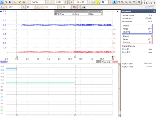
In the Overview you see frame_in in the master on D14 and frame_out in the Slave on D10. Both have a delay from 10.95 µs,
that is the length of the synchronization pattern + the transmission time.
After zooming you see a jitter from only ~ 30 ns on the frame_in on slave, though the source of the signal is in the master
and the full transmission via SPE is between both. That is less. See ..\SpeA-FPGA\SpeA-JavaFPGA.html##ClkSync_Mdls.
There is described that the internal working clock (CE signal) is synchronized, so that the jitter is minimal.
With the frame_out as input to the controller either an interrupt to process the data can be start.
Or better, an internal PWM can be controlled by a PLL (Phase Look Loop) algorithm, see next chapter.
See chapters:
The next slave stations in the Ring receives the SFD in a exact related time with less delay, because the telegram is immediately forwarded in hardware. Only an additional jitter is added again, so that the jitter in compare to the master is now ..50 ns. This may be only prevented by an synchronization of the internal clock itself. In the yet given solution only the CE signal is synchronized, hence the internal non synchronized clocks of 10 ns in any station produce this non preventable jitter. But this jitter is low (50 ns vs. 50 µs cycle in the second slave, till … 300 ns jitter in the 10th slave).
The accuracy of the PLL control depends on the timer resolution in the microController and produces also a jitter in this range, see PLL control of the interrupt cycle
With a common cycle also it can be done:
-
The average time for Measurements should exact follow this cycle. For Measurements always the middle value (average, integral) of the pre-period should be used as characteristic of input signals, not a accidently time for a fast measurement. This is necessary to suppress technical noise which is usual synchronous to the actuator period (from a PWM), or also, to suppress accident disturbance with a higher frequency as the measurement one.
-
A PWM (Pulse Width Modulation) often use for output of data, for example Firing pulses for power valves or also simple outputs should work exact synchronous in this cycle to refresh the current data in each cycle.
2.1. Standard time stamp approach ? Or time in synchronized cycles
For Ethernet with >= 100Mbit/s there is a NTP "Network Time Protocol" (https://en.wikipedia.org/wiki/Network_Time_Protocol) or better PTP (Precision Time Protocol) (https://en.wikipedia.org/wiki/Precision_Time_Protocol) can be used, accordingly to the TSN (Time Sensitive Network) rules (https://en.wikipedia.org/wiki/Time-Sensitive_Networking).
But this technologies works only for the connections >= 100 Mbit/s, because they are not regarded in the original Ethernet 10 Mbit/s topology. The problem of the originaly 10 Mbit/s Ethernet was: The time of transfer of a telegram depends on the status of the line. For the line a Bus Topology is used. It means all station attacks the line. It is deterministic for transmission in a time range in milliseconds, regarding displacement mechanisms, but not for exact time stamps. Due to the presence of the star topology with its continue data stream, which can work with TSN and PTP, a proper time synchronisation for the 10 Mbit/s where never developed.
Now with SPE also the Bus Topology is in focus, with the so named "Multidrop Technology", and that does not support the time synchronization yet and per default.
But, the Ring Topology offers another approach for Time Synchronization:
-
Prior, not the time stamp should be offered to all stations as accurate as possible, but:
-
All stations should work synchronous.
It means the stations in the ring have the same time, but they don’t know (need not know) the exact absolute time. They work together, out of a global time.
It is possible to insert this stations in a global time (UTC, master clock etc.), but this is task only of the master in the Ring Topology. The master can do so by using one of the possible approaches: Standard Ethernet with TSN and PTP or NTP, or specific variants of SPE (with higher bit rates and Star Topology), which also supports TSN, NTP, PTP. Then the master can forwarding this absolute time in the Ring to all other stations with the Ring Cycle Synchronization, described following.
2.2. PLL control of the interrupt cycle
The solution of PLL control is individual for different controller. The principle is:
-
Measurement or capture of the time where the
frame_inis occurring, as relative time related to the currently counting interrupt timer. -
Comparison of this time information with the expected time. This is very simple if the interrupt is forced by the same timer.
-
Adjusting of the timer for the interrupt due to the measured difference. Whereby not the exact measured difference should be used for the new value. This is a simple P-part-controller. It is better to have a real PI controller (Proportional and Integral Part) which is changed by the time difference as input. The output can be used as reload value for the timer, which generates the interrupt.
It means while PLL controlling the interrupt cycle is a little bit lesser or greater, not constant with the same reload value. A constant cycle has usual not the same time as in the master cycle because of quartz frequency tolerances. It would run away by accumulation of time. Hence the time should be adjusted sometimes a little bit.
                   !                       moment of the frame_in
..0..........987654321.................... timer count value
                  +                        expected moment of the frame_in
In the shown situation the next cycle should be 1 time longer so that the expected moment and the occuring moment of the frame_in
should be better matching. But the following cycles may be the same again, but in the mid value a little bit longer
to prevent furthermore abbreviations.
If for example the frame_in comes with a cycle of 50 µs with the quartz of the SPE-Ring-Master,
with 5000 steps of a 10 ns internal clock,
but a slave has an abbreviation of the quarts frequency from +0.001% (10 ppm),
then is should have ~5000.05 steps. It means, 19 times 5000 steps and 1 time between 5001 steps for the interrupt counter reload value.
It results on a jitter of ~ 10 ns, but an exact synchronization.
Because the measurement has also a resolution of this 10 ns, the value is not exact,
it results last not least in a little bit greater jitter of maybe 30 ns (as experience).
If the clock frequency or the frequency of the appropriate counter and capture units are lesser, for example 20 MHz resolution (50 ns steps),
the resulting jitter is in range of ~150 ns.
This counters may determine also sample and integration times in hardware or Pulse Width Modulation (PWM) times. In comparison to the 50 µs cycle this is a inaccuracy in range of < 1% jitter, but a higher accuracy over more cycles (related to middle values), hence acceptable.
Todo idea that the capture and control is part of the FPGA!
Old text:
The different length of an interrupt cycle is a jitter between the Ring cycle (telegram cycle) and the internal timer and interrupt. The range of this jitter depends on the resolution of the timer. If the timer both for interrupt and capture runs with 10 MHz only (100 ns), then the jitter is of course > 100 ns. Because of some small inaccuracies the jitter may be in range of 300 ns. This is added to the telegram jitter (from 30 ns in the first station to 300 ns in the 10th station). A sum of 600 ns jitter for a 50 µs interrupt cycle is not too far. But for analog measurement and also for the PWM output this can be on a limit.
Another possibility for synchronization of the controller with the Ring cycle is:
Using a Clock output signal from the FPGA caused by the internal central CE clock as clock input
for the processor. Processors sometimes have a PLL for the internal clock to generate a higher
clock frequency from a Quartz with lower frequency.
Measurement the time of frame_in should than be used only for the first synchronization
and also for checks.
For this solution it should be known that the 10 MHz or 5 MHz clock output can have abbreviations from the constant frequency because of the clock synchronization, see link:../SpeA-FPGA/SpeA-JavaFPGA.html#RxClkSync>> in the FPGA itself. The CE period switches between 9..10 internal clock periods (90..100 ns) or between 10..11 (100 .. 110 ns). This unrest should be processed by the controller’s PLL.
Hence the best solution is: The FPGA clock itself does not come from the Quartz, it does come from a PLL in the FPGA. Then each FPGA can be synchronous to the master’s quartz frequency. And also, the controller in the master is forced by the FPGA quartz or vice versa (maybe better). Hence only one quartz frequency exists in the whole ring. All is synchronous in one ring. Another related ring can be used also the same controller quartz if it is mastered by the same controller. This is the best solution of exact cycle synchronization.
Because of the cycle synchronization so far as possible all stations have the same time, independent whether they use (and knows) the time stamp itself or not.
3. Data exchange between the application in the controller and the FPGA via SPI
For the data exchange between an Ethernet adapter (its PHY chip) and the controller often SPI is used ("Serial Peripheral Interface"). SPI is familiar for all controller. This is also the solution for the SpeA-card.
Usual standard PHY/MAC chips have an internal memory for the data, the "telegram stack". Data for transmission are first written via SPI with any baudrate in the MAC chip telegram stack (MAC = "Media Access Interface"). Then, depending of the state of the transmission line or switch, the telegram is transmitted by the MAC/PHY chip independent of the controller. The same is for received telegrams, firstly stored in the telegram stack of the MAC. Then read out any time later from the controller via SPI. In this kind the telegram transmission is decoupled from the controller activity, but the communication is also delayed. For example a PHY/MAC typical on a PC can receive and store 600 Telegramswith 1.5 kByte received with 1 Gbit/s in the internal telegram stack, and later read out in a cycle of 10 ms by a program running on PC. The decoupling of SPI transfer and Ethernet telegram transfer is an advantage for the controller software, it is independent. For example the controller may be slow (lesser than 10 MBit/s for SPI transfer) but the Ethernet is fast (100 Mbit/ 1 Gbit). But with this approach only transfers in Millisecond range can be done.
This SPE solution takes another approach: "data just in time". In opposite to the common known solutions for Ethernet adaption to controller, this SpeA-card (its PHY/MAC, the FPGA) usual does not store the data internally.
3.1. Data just in time approach, principles
The data are immediately "on the fly" transmitted from the RAM to the SPE telegram output, and also immediately written to the RAM while receiving. This approach requires supporting a boud rate for SPI from the same as the telegram, it means 10 Mbit/s. The second one necessity is: The SPI and DMA should be prepared before a telegram comes in. It means the controller software (in interrupt) should be oriented to the telegram flow. But exactly this is desired for a strong cyclically communication.
Hint for a 100BASE-T solution: This requires either a SPI baudrate of also 100 Mbit/s which may be supported by fast controller solutions, or a parallel access to the RAM (160 ns/16 bit should be possible). For slower controllers as slave on the 100BASE-T ring only a few words should be received and transmitted temporary stored in the FPGA. The amount of forward transmitted data in the ring topology does not need a controller access.
The just in time approach enables communication and reaction in microsecond cycles with less additionl delay.
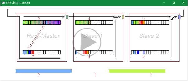
An example how does it work is explained as text in the following linked article (click the picture), needs 2 MByte to load. This article contains also a link to a video.
For that the solution for SPI is: The SpeA-card acts as master for the SPI communication, the controller is the slave. The controller prepares the access, whereby DMA should be used, but the SpeA-card determines the timing of the SPI access.
Additionally, especially for configuration data, or for a simple controller in an SPE-Ring with less data communication, the controller can access the SpeA-card also as SPI-Master, the SpeA-card is then the SpiSlave. This can be used also for data communication if the controller is slow (does not support 10 Mbit/s SPI or has DMA possibilities) and the station is Slave in the SPE-Ring topology. Then most of the data are transferred from the Rx to Tx in the ring, independent of the controller. Only a few data which are stored internally in the FPGA are exchanged with the controller.
3.2. Reset State of the SpeA card
The SpeA card is not automatically reseted if the control is reseted and vice versa.
If the controller comes out from reset, it should be firstly program the SpeA card with SPI master access.
This should determine completely the internal state of the card independent of the state before.
In that time the signal frame_in should held passive low.
If the SpeA card was reseted, but the controller works furthermore, the SpiMaster access from the SpeA card is not done.
This situation should be detected in the controller’s cycle, by testing the SPI register states.
The controller should then start a new initialization phase of the SpeA with low inactive frame_in signal.
If the SpeA card was reseted and the controller accesses the SpeA card by itself as SPI master, it reads out the bit bSet as 0.
See Mode bits in configuration. Then a new initialization should be started in the controller.
A SpeA-card which is not connected to the controller, or the controller is in reset or crashed after reset, the SpeA-card works proper as SPE-Ring Slave. See the default mode bit states in Mode bits in configuration This is important because the communication in the Ring should not depend on the proper work the software in any station in the ring. On faults the ring should primary work.
Only the dedicated master in the ring can be determined by hardware to prevent this SPE-Ring Slave forward transmission. This is necessary because otherwise a life of its own can occur: A telegram can be generated and circle continuously in the ring. The master functionality breaks this forward transportation, and the ring is silent if the master is silent.
The hardware determination for master is a jumper (connection) between J3.9 (FPGA pin A16) and J3.10 (GND).
3.3. Set the configuration with SPI master access from controller, especially after reset
Without using the frame_in signal, held it inactive low, the SPEa-card can be accessed for all configuration and data register via SPI,
whereby the controller is master of SPI, the SpeA-card is slave.
A complete overview over all mode bits in the configuration is given in SpeA-ControllerSw.html#SpeA_FPGA_ModeBits
-
The card can be switched as master or as slave for SPE transmission independent of the hardware determination on jumper J3.9-10. It means a predicated master can programmed as slave and vice versa. This is necessary for tests of connection. Mode bit
txMaster(9) -
The SpiMaster access from the SpeA card should be enabled if necessary. Mode bit
enSpiMaster(8) -
The mode of transmission can be set, with or without gap. Mode bits 11,10:
txNoTristateInGapandringNoGapMin. The first one is active for a master telegram transmission (with mode bit 'txMaster'). It assures the after the telegram immediately (after a short break) the sync pattern is transmitted, the line does not go in high impedance state. This mode is possible for the ring communication, it saves time and allows more data words in the telegram (max. 41 for a 50 µs cycle or 29 in a 31 µs cycle).For a SPE-Ring-Slave set of
ringNoGapMinis sufficient because then, the sync pattern from the station before forces immediately transmitting also the sync pattern. If the bittxNoTristateInGapis additionally set, this station transmits always without gap, also if a gap is received.The default mode (for SPE-Ring-Slave) is
ringNoGapMinbut nottxNoTristateInGap. Hence the station follows the received telegram. -
At last the
bSet(15) should be set. This bit is cleared on hardware reset, so the hardware reset situation can be detected.
3.4. Behavior on transmission collision
The transmission level on the output pins is anytime read back and compared with the transmission level (with a small disable range on the edges). If the read back level is faulty, then an internal flipflop is cleared which forbids further output. It means this station switches off its transmission activity. If other stations do the same, then the line is fast in high impedance state after a collision.
The flipflop can be read out with the bit txCollision (14) in the mode config word. What to do depends from the software.
In Ring topology this can occur if two stations transmit, using the opposite plug. Then one of the station, or both, are faulty configured.
In bus (multidrop) or star topology this can be occurred as normal situation if the participation on the bus is not clarified. Then usual the transmission should be repeated after a randomize time.
An adequate situation is given if the card is configured for transmission, or it is in state of configuration, but the transmission has not yet started. Then no collision occurs, receiving data, a carrier signal, comes. Then the same bit is set.
To detect such situations, the following flow is used:
-
On start of SPI access either for transmission or for receive preparation the bit
activated(13) in the mode config word should be set. After detection this bit in the FPGA the collision detection for transmit and the carrier detection for receive is enabled. -
If the mode for
txMaster(9) is set, then a received carrier on the selected transmission channel (bittxSlot2, 12) is a collision though the transmission has not started yet, the bittxCollisionis set and the transmission is not started. -
But the received telegram is written via SPI in the RAM, so it can be evaluated.
TODO
3.5. Timing and Programming SPE Ring Master
See also SpeA-Manual#SpeRingFast
Before this procedure starts, the SpeA card should program in its mode bits as:
enSpiMaster = 1;
txMaster = 1;
txNoTristateInGap = 1;  //recommended
The controller should organize a cyclically frame_in signal for the SpeA-card usual from a timer or a PWM (pulse width modulation) output,
see Chapter Provide the frame_in signal to the SpeA-card, process the frame_out.
Such modules are often existing on controllers.
The frame_in should have a long high period, so long as the telegram runs, and a short low period. For example 45 µs high and 5 µs low.
The FPGA is the master for the SPI communication.
In the low period of frame_in the controller should prepare the SPI interface as slave.
Using DMA is strongly recommended, this DMA should be prepared with the expected number of words to read and write.
Immediately after the falling edge of the frame_in Pin the FPGA starts reading and writing 3 x 16 bit from the controller.
This first three words are a command word, a config word and the first data word.
Then more data words (á 16 bit) are read in the timing of transmitting and receiving data bits from SPE just in time. See chapter ../SpeA-Manual/SpeA-ControllerSw.html#DataExchange. This forces a small gap between the first three words and the following. The SPICLK is determined by the internal clock of the FPGA.
The following fast image should show the timing of interrupt, SPE telegram and SPI access:
PWM:  ++|__________|++++++++++++++++++++++++++++++++++++++++++++++++ The PWM output for frame_in
Intr: --ccciiiiiiccccccWWWccccccccccccccccccccRRRccccccccccccccccc-- one cycle interrupt
SPI:  ________________ccff11 ddRRRdddWWWdddddrrrddddddddddddddddssss
SPE:  yyyyyyyyyyyyyyyyyyyyyy11ddRRRdddWWWddddddddddddddddddddddCRC_yy
-
|___|should present the hardware signal forframe_in, be carefully with the moment of edge. -
The
cccshould present any statements of the cyclically interrupt -
iiiare the initializing statements for SPI, programming FIFO and/or DMA. -
WWWare data which are calculated on the fly for transmitting, possible -
RRRare data which are used on the fly from the SPE communication -
ccff11are the first three words, command, config, first data word -
dddother data. -
yyySynchronization pattern of SPE
As you see in the simple schema, the interrupt starts with the falling (trailing) edge of frame_in.
Firstly the SPI should be prepared, before the leading rising edge of frame_in comes.
After the leading frame_in first the command, config and the first data word are gotten from the controller via SPI.
Then the SPE telegram starts with data, transmits first the first data word.
During transmission, the interrupt can prepare yet still data, which are transmit in the immediately following time. For that the calculation times in the interrupt should be well known. But often this is possible. This is the 'data on the fly' approach. The even yet processed data are a small time afterwards transmitted.
The adequate same is with receive data. Data which are already received and written in the controllers RAM, can be processed immediately after. If such received data comes on the start of the telegram, whereas the new data to transmit on end, there is enough time.
With this approach the dead time for a closed controlling loop can be reduced.
The opposite variant is: Using a alternate buffer for transmitting and receiving. Then the data in the second buffer can be full prepared or evaluated while the other buffer is currently used for SPI. This forces one step time more as dead time in a closed loop solution. But the preparation and communication is independent.
3.6. Timing and Programming SPE Ring Slave - interrupt for SPE—Ring-Slave
If the SpeA-card works as SPE-slave in Ring Topology, then the first three words should be initialized as necessary. A receiving telegram can be expected due to the whole communication timing, but it is forced from the transmitting station before. A received telegram is immediately forwarded in the Ring as transmission.
If the interrupt in SPE-Ring-Slave controller is forced by the frame_in signal comming with the SFD,
then the SPI communication should be already initialized. Also the first two words should be read from the controller RAM.
It means, this should be done on the end of the interrupt before.
In the moment of starting the interrupt, the first data are written via SPI to the controller RAM already. This should be done usual with a DMA related to the SPI. It means, new data are written now.
If the interrupt has some preparations which needs a dedicated small time, and the information to use are on start of the telegram, the interrupt can access the just now written information immediately after writing in the same interrupt. If the relevant informations are a little bit later in the telegram, some other things may be done firstly. It is only a quest of 0.8 µs per byte.
It means there is no additional dead time in controlling loop. The new received information can be used in the same cycle.
But there is the following problem: The check via CRC is not done till now. It means either you wait till the end of telegram to get the result of CRC check, or you can calculate new values with the non checked information first, but discard this information on the end of the controller algorithm if the CRC is faulty. It depends on the controller algorithm. Usual it is not recommended to stop all functionality on one faulty telegram. It is better to replace information with estimate values, because the accident of an error is less. If one step produces non exact outputs, and the next step in a controller algorithm is exact again, it is only a small disturbance. On a fast cycle time this disturbance is not so problematically. The important one: You should not switch a state because one unexpected signal. If you switch a state, you should leave this state again if the next step is proper, as expected.
Look on the following schema:
 ssssSdddddddd.....dd_crc________________ssssSddd     The telegram
     !ppppppp_ccccccccc_pppp_ooooiiii        !pppppp  The interrupt
In telegram:
* ssssS the synchroniation bits, and the Start Frame Delimiter
* dddddd receive data and write to RAM immediately
* crc Receive the CRC check sum after data
In interrupt:
* ! start of interrupt
* p do any other unrelated to telegram data (preparation, any what)
* c calculation of the controller algorithm with the yet immediately received data
* o Output results, after CRC check
* i Intitialize SPI communication for the next cycle, write first two words.
As you see, the intitialization of the SPI should be done if the telegram has finished. But this means that the interrupt should be run longer than the telegram. This may be proper if the controller has its main task execute the interrupt, and the calculation time is ~70—90 % of the cycle time.
3.7. Timing and Programming SPE One shot Master
This procedure is proper for either an answer in Bus- or Star communication after receive, or for test situations.
Usual, with SpiMaster mode of the SpeA-card, first the leading rising edge of frame_in is output.
Because of the txMaster bit was set = 0 before, this does not start the active output yet.
But the SpiMaster access starts and reads the following mode bits:
enSpiMaster = 1;
txMaster = 1;
txNoTristateInGap = 0;   // use the gap in bus mode
ringNoGapMin = 0;
activated = 1;
bSet = 1;
Because of now the txMaster is set, the transmission starts immediately with the programmed number of sync bytes.
Following, the data are read and transmit. Because of the sync phase there is a little bit greater gap between the SPI accesses.
After transmission the activated is set to 0. The txMaster remains 1, but without new initialization nothing will be transmitted.
The next
3.8. Timing of SPI data transfer with frame_in - PLL interrupt synchronization for SPE—Ring-Slave,
On the slave the timing should be similar. But not the step_in is the trigger,
the data comes with receiving a telegram.
Exactly therfore SPE-master and SPE-slave should be synchronized in the cycle time,
see chapter Cycle Synchronization approach. Then the receive telegram does not come unexpecting,
it comes in the expected time range.
Before the receiving is expected, also (as in SPE-master) the SPI interface of the controller should be initialized. All other is adequate.
3.9. Data on the fly
As shown in the graphic it is possible to write data for DMA transfer a little bit shortly before they are read from SPI to transmit. The same is with receiving: Using immediately after receive.
But this requires that the timing both from machine code execution in interrupt and the position of data in the SPE telegram are known, stable and tuned. For some simple controlling applications this can be done (need constant calculation time, less jitter). Hence the dead time in the controlling cycle can be reduced. But this is a possibility which can be used in response to the application. You should also regard, that FIFO data should be written (and hence known) before the telegram starts, only DMA data can use this possibility.
In all cases it is not possible to handle the SPI data in software. For that the data rate is too fast (10 Mbit/s, 1.6 µs for 16 bit).
For receiving it is similar. Using a FIFO the first data are written in the FIFO, but some times the FIFO size is too small, and the FIFO is entlees via DMA to the RAM. Then this just in time data can be used. For just in time performance either no FIFO capability should be used or with less size. The DMA should be prior and fast enough for 1.6 µs per access (16 bit SPI access, 10 Mbit/s).
3.10. Meaning of the data words, Headerfile
ccc
3.10.1. Overview all configuration words
This structure describes the configuration data in the SpiData module in the FPGA.
The order is sorted to the index addrCfg in the cmd word.
The index should be given for writing in bits 15..12 of the cmd (first SPI data word after leading edge).
The following data word for SpeA-card SpiMaster (Controller as SPI slave) is the only one data word.
For SpeA-card SpiSlave (Controller as SPI master) more words can follow with incremented indices.
//SpeA_Common/SpeA_FPGA.h:
typedef union CfgData_SpeA_FPGA_T {    // it is a union:

  uint16 words[16];                    //:  access to the data as array.

  struct words_CfgData_SpeA_FPGA_T {   //: structured access
    uint16 data0;                      //: @0: yet unused

    ModeBits_SpeA_FPGA_s mode;         //: @1,2: 32 Mode bits, see type definition

    int16 data[7];                     //: @3: 7 data words for the SPIslave mode to transmit and receive.

    /**4  */
    SelTest_SpeA_FPGA selTestRx        //: @0xa..0xe: words for test output selection
                    , selTestTx        //: from the FPGA internal signals to three test pins.
                    , selTestSpi
                    , selTestAux1
                    , selTestAux2;

    uint16 addrDataSelectSlaveSpiToTx; //: @0xf: Write word to configure the RAM for selction slave data to Tx
  } w;                       // the config words
} CfgData_SpeA_FPGA_s;
3.10.2. Cmd bits in the first 2 words of any newly started SPI transmission
A newly started SPI transmission is given after a frame_in signal from the controller to the SpeA-card,
if the SPI on the SpeA-card is master (controller is slave)
or just with a first SPI access from the controller as SPI-master after a falling edge of the frame_in
(comes from active to inactive) maybe as reset impulse for SPI master transfer.
This first two words contains always a config word which updates the internal configuration.
Especially the first mode bit can be updated immediately on start of a datagram.
Then the bits addrCfg should contain the value =1.
//SpeA_Common/SpeA_FPGA.h:
typedef struct SpiHeadBits_SpeA_FPGA_T {
  union Cmd_SpiHeadBits_SpeA_FPGA_T {
    uint16 w;                          // access to whole cmd word.
    struct CmdBit_SpiHeadBits_SpeA_FPGA_T {
      /**Number of data words to transmit -3. max. 750 words are necessary for a 1500-Byte-telegram. */
      uint16 nTx: 10;                  // 9..0

      /**Read and write the master state for SPE-tx.
       * On hw-reset the master state depends on the connection J3.9-10 (connected to GND: this bit is 1)
       * This bit should be set =1 or =3 if a telegram should be initiated from here.
       * if set =3 then transmit the next telegram with coming frame_in after the dedicated frame_in time.
       * The synchronization phase starts immediately after frame_in.
       * The reading of the first 3 words via SPI are executed during the initialization phase.
       * Set =1 if it is only a single not cyclic telegram.
       */
      uint16 txMaster: 2;                //11..10

      /**Address which config word should be written as next.
       * Only one cfg word will be written per cmd word. */
      uint16 addrCfg: 4;               //15..12
    } b;
  } cmd;
  /**Second word in telegram is always a config word for the FPGA.
   * Its index (address in data) is determined by cmd.b.addrCfg */
  uint16 cfgWord;
} SpiHeadBits_SpeA_FPGA_s;
3.10.3. Mode bits in configuration
The mode bits are assembled in two data words a 16 bit. The first word contains mode bits, which may be changed in a specific way for a just transmitted or received telegram. The second word contains bits only for configure.
//SpeA_Common/SpeA_FPGA.h:
typedef struct ModeBits_SpeA_FPGA_T {

    /**transmit the FLP in a cycle of 16 ms if not traffic on Tx is given.
     * 0 - disable 1 - enable Tx1, 2 - enable Tx2, 3 - enable both similar.
     */
    uint16 enTxChnNFlp : 2;
    /** bit 2=1 (4..7): transmit the TLP pattern, =0: transmit only a 16 ms NLP pulse.
      */
    uint16 flp_pattern : 1;

    uint16 flp_Ackn : 1;

    uint16 spare1 : 4;

    /**Write and read back: 1=Enable the SpiMaster access from the SpeA card, default is 0-disable*/
    uint16 enSpiMaster : 1;        //8

    /**Only if this bit is set, receiving will force SpiMaster access to the controller.
     * If also txMaster is set (bit 9), then receiving a carrier without transmission
     * sets the txCollision bit but received data are written via SPI.  TODO was not used last times
     */
    uint16 spare9: 1;             //9

    /**Write/Read back
     * 1=A minimal time for a gap (high impedance line) is not regarded.
     * Then a received telegram in ring is immediately forwarded with Sync-Pattern
     * if a carrier (with sync pattern) is received.
     * 0=Transmission is delayed till the minimal time for a gap (high impedance state) is expired.
     * Because of a Slave Telegram in SPE-Ring is immediately forwarded, too fast telegrams
     * have then either a shorter sync phase, or starts without sync, which is faulty.
     * But the problem is the too fast telegram transmission in the ring, not this bit.
     */
    uint16 ringNoGapMin: 1;        //10
    /**Write/Read back
     * 1=Instead a gap sync patterns are transmitted immediately till the next telegram starts.
     * This reduces the loss time in a cycle in a fast ring communication.
     * 0=after finish a telegram till the next telegram request the line goes in a high impedance state.
     * This is the gap. Note, that if a telegram in the SPE-Ring is received with sync pattern and forwarded,
     * then it is the next telegram request already, the behavior depends then of the bit ringNoGapMin.
     */
    uint16 txNoTristateInGap: 1;   //11

    /**Write/Read back: 0=transmit via Slot1 (left from front view), 1=use Slot2, right side. */
    uint16 txSlot2: 1;             //12

    /**If this bit is set, the Rx is echoed on tx if it is not the SpeMaster. */
    uint16 rxTxEcho: 1;            //13

    /**Read 1=Tx is disabled because of collision detection.
     * Write 0=hold the state disable or not, 1=reset the disable state to enable. Quit disable.
     * On disable the state should first recognize by reading without enabling, set usual to 0.
     * Only if a disable state should be quit, write here a 1-bit.
     * The tx disable state is also valid for a SPE-Ring-Slave.
     * After hw-reset the txDisQu is false, no disabling.
     */
    uint16 txCollision: 1;             //14

    /**This bit is 0 after reset. It can be set to 1, to detect a occurred reset on the SpeA card*/
    uint16 bSet: 1;        //15

    //word 2
    uint16 nTxBreak: 5;             //: 4..0: bit pattern time for break the telgr after CRC
    uint16 nSyncBytes: 3;           //7..5
    uint16 spare2_8: 8;

} ModeBits_SpeA_FPGA_s;
3.11. Received data, meaning
The received data are written via DMA to the RAM. The first two words contains the own command and sender, then received data with the sender address follows. Between both they may be fill words with content 0000 on the SPE-master if the response time in the ring is a little bit greater.
5. Endian approaches: Ethernet Big endian LSB first, SPI: word access, MSB first
But the output on SPE is defined adequate to the Ethernet standard with first output the LSB, but from the high byte of the 16 bit access (big endian approach).
The big endian approach should be correct understand: If a memory word (16 bit) is accessed, the processor reads the memory word correct. There is no endian approach for reading whole words from memory, endian approach is only existing for serializing of a word. It means the 16 bit access for a 16 bit word is always correct independent of endian thinking.
But for a 32 bit word, which is accessed by two 16 bit reading from SPI,
first the bits 31..16 should be accessed from memory to transmit exactly first bit 24..31 and then bit 16..23
via Ethernet SPE. Following with access bits 15..0 via SPI to transmit bits 8..15 and then 0..7 via SPE.
To do so, it is necessary to reverse the content in the memory.
This is similar the known hton and ntoh operations "host to net" and "net to host".
But, for approaches of fast data transfer often only 16 bit are used. The order of word remains independent of big or little endian accesses. And, if both partner accepts a 32-bit or longer word without word swapping, it is also okay. The swapping is only necessary if the information are evaluated in an unknown or common way, then the big endian approach is valid and should be recommended. This is an effort in software, not in the PHY layer of this FPGA.
Examples to explain the big endian approach:
 //data example:
 int16 data = 0xabcd;
 int16 datb = 0x1234;
 int32 dat32 = 0xfe0a5678;
Memory content:
  cd ab 34 12 78 56 0a fe      content in memory as byte width for little endian approach
  abcd  1234  5678  fe0a       content in memory 16 bit width for little endian approach
  abcd  1234  fe0a  5678       changed content to transmit for big endian approach
  ab cd 12 34 12 fe 0a 56 78   Transmit order, transmits LSB of each byte first.