1. Approach
This FPGA design is usable for SPE communication with 10 Mbit/s and Manchester-2-coding either for Ring Topology or also for Star or Bus (Drop) Topology. Especially the Ring Topology is supported. The Bus or Star Topology is able to use too. It is the physical layer.
The data are not stored in this physical layer. Instead the data are immediately read and written via SPI communication. The SPI communication should be work with 10 Mbit/s.
For Ring Topology the frequencies and the phase of the Bits of the Telegram are tuned,
so that a minimal jitter is occurred.
This is also necessary for a exact time synchronization of all stations in the ring.
The time synchronization is done with the time of the Start Frame Delimiter (SFD)
after sync bits on start of the data. This timing signal is outputed as frame_out.
For the Ring Topology the FPGA can act als Master or Slave.
-
The Master starts the communication with the
frame_insignal. It requests data via SPI after them. The SPI should be initialized beforeframe_incomes. -
The Slave should be initiated also with the
frame_insignal. It reads two data words (32 bit) via SPI from the controller as command and sender identification. Then the FPGA waits for receive data. If a telegram is receiving, it is transmitting similar forward via the second SPE output. In that time the SPI is used to write the receiving data and also to read data which can replace data for the forward transmitted telegram. The replacement can be controlled for any byte of data by a configuration word. -
The Master receives data via its second SPE pins. That is the answer in the closed Ring.
2. SPI data transfer, general timing
The controller is connected to the SpeA-FPGA via SPI, either as Slave, the FPGA is master, or as Master (FPGA is Slave). For fast data transmission the Controller need work as Slave, because the FPGA determines the timing of data access. For that the controller should support 10 Mbit/s SPI access.
2.1. FPGA as SPI master, SPE master, timing
The controller sends a frame_in signal. This can organized by a Timer output with a constant period and a dedicated pulse width.
Immediately after the falling edge of the frame_in Pin the FPGA starts reading and writing 2 x 16 bit from the controller. Of course the controller should be prepared. DMA is recommended to use, this DMA should be prepared with the expected number of words to read.
Then more data words (á 16 bit) are read in the timing of transmitting and receiving data bits from SPE just in time. See chapter Data exchange between the application in the controller and the FPGA via SPI. This forces a little gap between the first two words and the following. The SPICLK is determined by the internal clock of the FPGA.
If the FPGA works in Star or Bus Topology then it is always Master.
The time of answer is determined by the controller, which initializes the SPI
for the data transfer and outputs the frame_in signal to start the telegram.
3. Meaning of data via SPI in the controller
3.1. cmd word
The first data word (16 bit) read after frame_in is general a command word. It is not transmitted. This command word determines whether the FPGA is master or slave, if it is not set as master per hardware wiring (master input).
-
Bit 15: should be 1 if SPI provide this.
-
Bit 14: 1=Tx on Slot2, 0=Tx Slot1
-
Bit 13: 1=master
-
Bit 12: 1=continues carrier for Ring, 0=no tx bits in gap, for Bus topology
-
Bit 11: 1=Special meaning, configuration word (not yet ready)
-
Bit 10..0: Length of the data (without CRC, without first 3 words) in 16-bit words. It means for Bit 10..0 == 0 three data words + CRC (4 bytes) are transmitted.
3.2. first data word
The second data word is transmitted. For the Slave in Ring topology only the hi-byte is determined before receiving bytes are evaluated. Hence is is never echoed from receiving data.
The first data word will be transmitted always from the master. For non-Ring Topology the station is always master.
Only for Ring Topology a Station (FPGA) can be used as slave. Then the following is valid:
-
Bit 15..8: Sender identification, it should be evaluated by the next station.
-
Bit 7..0: Data length for the next station to forward the data. This data length information is transmitted from the Master from RAM, and forwarded from all slaves. It is necessary to determine the data length independent of the slave programming, because in the initial phase a or on fault a slave controller may not work.
3.3. more data word
All other words are user-free. The data content of the telegram is determined immediately by the RAM content in the controller.
For the Slave in Ring topology a configuration phase determines which bytes are gotten from the RAM of the controller, and which bytes are forwarded from received data.
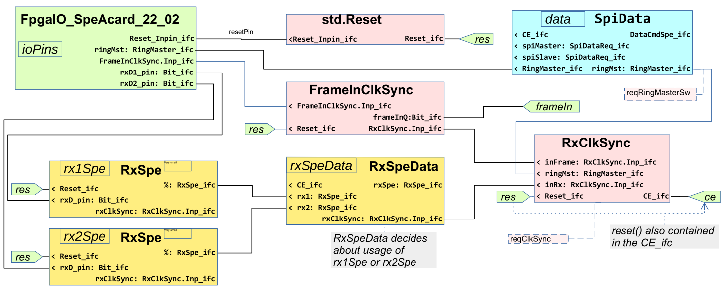
4. Moduls
4.1. All moduls
todo Graphic
4.2. RxSpe preparing the receive data input from SPE
The Module SpeRx is responsible to evaluate the difference signal input immediately from the received signals.
A first task is suppression of noise:
-
If the line has no signals, accidently disturbance in mV-range causes an input signal.
-
Reflection on the line (signal transmission) can force additional edges in the signal.
-
A less signal level (long lines) increases disturbance by accident due to electromagnetic influences.
The second task is decoding the Manchester-Code and restore the clock: * The Manchester code has one edge per bit, but an additional edge if two bits comes with the same value. * The bit edge restores the clock. * The second edge should be detected and suppressed for clock detection. * The data should be identified with the correct edge.
The next 3. task is synchronization detection, detection of the Start Frame Delimiter, detection of the beginning and end of the data frame:
* Only if a stable signal for synchronization is recognized for a given number of bits (0 - 1 - sequence)
then synchronization is met.
* Two times the same bit value is the SFD (Start Frame Delimiter). Whereby depending of polarity it can be 1011 or also 0100.
* 1011 is the expected SFF (the second 1 after 1), 0100 occurs on a changed polarity of the line.
This is accepted, then all bits need to be negate.
* The SFD marks the position of the first bit of the first word, comes as next bit value.
The end of a telegram can be marked with a lost signal. * The end comes after CRC detection. The CRC check code should be 0 if the end is detected. * It is expectable that no more bit change edges comes. It means the end is detected with a longer signal level. * But because the lost signal offers an accident level on the line also no exact end may be detected, instead a faulty pattern by the bits. This is also okay if the faulty pattern comes in the time of 8 bits. Then the last calculated CRC value for a full byte is meaningful.
But for a communication in Ring Topology it is not necessary to have a gap between telegrams.
Instead, after the CRC it can be continued with a sync pattern.
* Then either it can be checked whether a calculated CRC value of 0 comes, and after them only sync bits.
* The end may be detected by a minimal given number of sync bits.
* Or the telegram length given in the head information in the telegram data is used to detect the position of CRC
in the data frame and after that the end. See signal ctDataCy
* But this task is not fulfilled by the RxSpe module. It is done by the RxSpeData module, see RxSpeData
The shifting of bits, counting the bit and word and detection of the end of the telegram frame without gap is done by the RxSpeData module, see chapter RxSpeData. The 4. task of the SpeRx module is
4.2.1. Inputs and Outputs
Input Pins:
=>source: java/srcJava_SpeA/org/vishia/spehw/fpga/RxSpe.java
The clr signal comes from a central logic in the FPGA, reset logic.
Of course in VHDL also the system clock is part of the input signals.
The rxDin should be immediately connected in the top level VHDL signal
from the non filtered and non clocked input pin, which is a difference input.
Inputs from other module:
=>source: java/srcJava_SpeA/org/vishia/spehw/fpga/RxSpe.java
  private static final class Ref {

    final Bit_ifc rxD_pin;

    /**True than all data are received after activating dataState via {@link RxSpe#dataStateRx()} was set.
     * This information come from the RxSpeData which counts the data words.
     */
    final Bit_ifc rxDataComplete;


    final Reset_ifc clr;

=>source: java/srcJava_SpeA/org/vishia/spehw/fpga/RxSpeData.java
The only one signal used from other module is the ctDataCy. If this bit is detected
in the data receive state, then the next data are CRC code.
Outputs to other module:
The following signals are interesting and provided for other modules in Java via interface. Note that the access in the hardware (VHDL) is done immediately to the adequate FF outputs. The names of the interface routines are exactly the same as the signal names. The interface is related to (the only one) sub module or VHDL RECORD in this module. The interface access offers the possibility for different supplying the signals in a test environment. If a module needs this RxSpe module to work, it is also satisfied with a proper interface implementation in the test bench. This is a proven approach for testing, also used here.
=>source: java/srcJava_SpeA/org/vishia/spehw/fpga/RxSpe.java
-
ceis the clock of the received data. It is used used to synchronize the Tx Clock of this module if it is the slave in Ring Topology. Then the centralCE0clock can be used for all. For the Master in Ring this clock is not synchronized to the centralCEclock. It means time delays to process the received data needs the originally 10 ns 100 MHz system clock. -
rxDis the received data bit after Manchester decoding. It is immediately forwarded to the TxSpe transmit data input to SPE module if the data are forwarded for Ring Topology. It is used also for the SpiA - interface to the controller module to store the data. Shifting is done in SpiA. The data are valid with the followingce. -
carrier: This signal indicates, a valid data stream is receiving on the SPE input. It is 0 if the SPE input stream is invalid. An valid stream has edges at least in the 100 ns bit width, with possible inaccuracies because of disturbances on the wires (cable). But no edges in a time of 150 ns and too much disturbances are indicated ascarrier_Out =0, it means no valid data. Note that a non driven line can force non deterministic data inputs, because the difference Input for SPE signals are sensitive. After a disturbance which forcescarrier =0at least some correct Sync Pattern bits should be come to indicatecarrier =1.Note that in Ring communication a non interrupted data flow is transmitted. It means
carrier =1is valid for the whole time of communication. This signal cannot be used as end detection of a telegram. See next. -
dataState: This signal indicates valid received telegram data.-
It comes
dataState =1after detection of the SFD (Start Frame Delimiter) as end of the synchronization phase, it is synchronized. It needs at least 32 Sync Bits.It goes (
dataState =0) either -
if a gap is detected (no data) in the received SPE data stream, also indicated with
carrier =0. This is used for Bus Topology especially for Multi Drop Communication -
or if the given number of Data words in the
cmdSpiis expired. This is dedicated if the inputctDataCygets= 1This is used for transmitting without gap in Ring Topology. To switch off this functionality for Bus topology the number of expected data words should be set to0x3FE. This is longer as the longest Telegram in Ethernet specification (0x3Fe= 1022 data words = 2044 Bytes).
Hence this signal is deterministic for the data phase.
-
-
negData: This signal is only used as test output, especially to show the negated data state on a Led. The SPE wires can generally connected also swapped. It means a transmitted Sync signal ends not with..0101011but with..010100. The SFD is not a11pattern but a repeating of the same bit value. Hence the swapped wiring is admissible. It is detect and regarded in the RxSpe module itself. It means therxDcomes with the correct value. But this state of swapped wiring may be interesting for the wiring itself, hence it is shown.
4.2.2. Detection of Bit edges and Databits
This is done in main/vhdl/modules/common/speA/RxSpe_SpeA.vhd by the
=>source: java/srcJava_SpeA/org/vishia/spehw/fpga/RxSpe.java
  @Fpga.VHDL_PROCESS Qrx(int time, Qrx z, In in, RxSpe mdl) {
  ....
      this.rxD0 = ref.rxD_pin.getBit();                    // clocked input unconditional
      if(ref.rxD_pin.getBit() == z.rxD0) {                 // Accept clocked input only if the input signal is still the same.
        if(z.rxD1 != z.rxD0) {                   // changed new input
          this.rxD1 = z.rxD0;                    // Note: Use FF output rxD0 as D-Input for rxD1, never the unclocked signal.
          this.time.rxD1 = time;
        } else {
          this.rxD1 = z.rxD1;
        }
      } else {                                   // but use rxDpin for Clock Enable check.
        this.rxD1 = z.rxD1;
      }
Firstly all processes use a RECORD Type to store the values of this process in states
respectively Flipflops (FF) in the real hardware. This record type is here Qrx_REC,
the Flipflop-Instance (Output values of the FF) is qrx.
-
The
rxD0is always the clocked input data pin. But: It is possible that the FPGA input pin has very short spikes. A spike can also gathered by the clock and elongated to 10 ns bit time. -
Hence in the next line
if(in.rxDin == z.rxD0) {compares the clocked input with the immediately input pin. Only if both are equal, then the stored pin before is valid. It means a short spike is suppressed already here. It does not come torxD1. -
The equate block
in.rxDin == z.rxD0is an asynchronous logical combination which is used to clock enable of only one FF, therxD1. If this signal may be hazarding due to the input signal. But if the combination is 1 in the moment of the clock edge, then it is nevertheless valid and used. That is either and in any case if the signal is really stable or it is a repetition of two spikes in the exact one clock period which is an accident or maybe influenced by EMC disturbance. But if such things happen all the time, then the signal quality is poor. -
It is important that this asynchronous logical combination is used only for exact this FlipFlop only. Elsewhere different delay times in the lines inside the FPGA causes undefined behavior. Thats why for the D-input of
rxD1the stable signal of therxD0is used. Thein.rxDinis only used for the combinatoric itself which provides only one signal, the CE input for therxD1.
That is the first important spike filter.
This is a simulation result (Simulink) with a hard disturb signal.
-
Track 1 is the input with disturbance as anlaog value.
-
Track 2 shows the situation after the digital input. Blue is the 10 ns clock. The signal itself seems to be unusable. All analog signal changes around here 1.65 V (in the simulation there is no difference input) produces binary signal changes.
-
Track 3 is the digital input after the first Flipflop, clocked with the blue 10 ns clock. The result in disturbance phases are accidently.
-
Track 4 is the CE building with the comparison
RxD0and Input. -
Track 5 is the binary signal after the correct
RxD1. It may be usable, because comparison of the input with the clocked input on any clock edge. -
Track 6 is the binary signal after the faulty
RxD1_bad, which uses the not clocked input on D. The problem is the different delays, here simulated with 1.3 ns and 2.3 ns. The simulation resolution here for this simple model is 0.1 ns.
The associated model is shown below:
Furthermore in this VHDL code snippet (not in the SImulink), a second qRx.rxD2 is used
to store the same signal as in Rx.rxD1 but one 10 ns clock later.
With both FF the edge of the input is detected.
4.2.3. Detection of Carrier, Sync pattern and Start Frame Delimiter
This is done in main/vhdl/modules/common/speA/RxSpe_SpeA.vhd by the
=>source: source: java/srcJava_SpeA/org/vishia/spehw/fpga/RxSpe.java[tag=detectInputSignal_Edge]
      else { // =======================                    // not clear
        this.rxD2 = z.rxD1;                                // shifted glitch filtered input for edge detection
        this.time.rxD2 = time;
        rxDchg = z.rxD1 ^ z.rxD2;                          //edge detection for change on input
        if ( rxDchg ) {                                    //=========== bit edge:
This is the Qrx process continued after clr-handling
Note that this document contains not all details, refer to the original source.
Only the contexts are explained. The source contains maybe sufficient comments.
The FF rxD2 follows rxD1, which is the glitch-filtered data input from the SPE line.
The rxDchg is a local variable in Java and a PROCESS-local variable in VHDL.
It is set to 1 if rxD2 and rxD1 are different, means the input signal is changed
on rxD1 and in the moment not changed on rxD2.
If an edge is detected, then the ctBitTime is checked:
=>source: source: java/srcJava_SpeA/org/vishia/spehw/fpga/RxSpe.java ... continued
          if(z.ctBitTime == 0b1101) {                  // bit time >= 0b1101 = 13, a too long bit:
            this.carrier = false;                      // this is the end of a telegram, start of gap.
            this.dataState = false;
            this.ctBitTime = 0b0000;
            this.ctSyncBits =
                0b0000000;
The ctBitTime is the relevant counter to detect the bits.
If this counter is at value 13 = 0b1101 then the time between edges is >= 13.
This is the first edge of the start of a new telegram with carrier and sync detection.
First it starts without the carrier signal and counts the sync bits from 0.
The ctBitTime starts of course from 0 again.
The value 13 is tuned to the clock frequency of 100 MHz = 10 ns and the nominal bit width of 100 ns. It means 9..10 clock edges is the nominal bit width, but 11 and 12 is admissible also. The signal on the SPE wires can be delayed depending on the signal levels up to the switching point on the input.
=>source: source: java/srcJava_SpeA/org/vishia/spehw/fpga/RxSpe.java ... continued
          else if (z.ctBitTime < 0b0111) {                 // bit time is between 1 ... 7 (z-value is <=6)
            if(z.carrier == false) {                       // for carrier detect, this is not a valid signal.
              this.ctBitTime = 0b0000;                     // a new bit time starts.
              this.ctSyncBits = 0b0000000;
              this.carrier = false;                        // remain false.
            }
            else {                                         // If the carrier is already detected, then
                this.carrier = z.carrier;                  // it is a signal change between the bit time usual to provide an edge in the same direction in a bit time
                this.ctBitTime = z.ctBitTime + 1;          // means a necessary intermediate edge
                this.ctSyncBits = z.ctSyncBits;            // do not count the sync bits.
            }
If an edge occurs in a time ⇐7 clock cycles = 70 ns, then it is not a full bit width. Such edges are necessary as intermediate signal switch to offer the same bit value in Manchester coding. The bit value is the direction of the edge after the full bit time. It means if twice time the same edge should occur then the signal should switch to the other level between. This is the basic of the Manchester coding.
If the carrier signal is false, then this is a faulty edge.
It means the carrier detection starts again from ctSyncBits = 0.
The edge is not recognized as intermediate edge.
Instead, the state before is detected as noise and this edge is interpreted as first edge of a beginning synchronization.
If the carrier signal is given, then this is either a real necessary intermediate edge to offer the same bit value outside the synchronization (data transmission, or the SFD), or it is a disturbance during the synchronization. Such an short disturbance can occur without effect on synchronization itself, as shown in the test results below. For the signal forwarding to the transmitter module the cleaned signal level is used.
=>source: source: java/srcJava_SpeA/org/vishia/spehw/fpga/RxSpe.java ... continued
          else { //ctBitTime = 8 .. 12                     // ctBit has the values 0x8...0xC, 0xA is the nominal one.
            this.ctBitTime = 0b0000;                       // then the next bit begins
            this.time.rxD = time;
            this.rxDs = z.rxD1;
            this.rxD = z.rxD1  ^ z.negData;                // databit with edge, the rxD1 is the state of the new bit value.
            Fpga.measTime(mdl.tgroups.rxD, 0, time - this.time.rxD1);
            if(!z.dataState) {                             // not in data state, it is in sync state, waiting for SFD
              if(!Fpga.getBit(z.ctSyncBits,4)) {           // count up the syncBits counter to detect sync pattern till max 0b10000 = 16
                this.ctSyncBits = z.ctSyncBits +1;
                this.time.ctSyncBit = time;
              } else {
                this.ctSyncBits = z.ctSyncBits;
              }                                            // the carrier is valid if at least one sync bit was received.
              this.carrier = Fpga.getBits(z.ctSyncBits, 4,1) != 0b0000;  //Note: do not delay carrier detection because from one of the next station the sync pattern will be shortened.
The else branch remains for the correct bit time between edges, whereby the shown range is accepted.
Then the ctBitTime starts with 0 to measure the next bit width.
The rxDs is the data bit value. It is sampled after an edge after the full bit width.
Because rxD1 presents the current level of input, the positive edge is an 1 bit.
This is an early time to detect a bit, immediately after a valid bit edge.
The rxD is the bit value regarding necessary negation.
The line with meastime is not related to the FPGA design itself (not translated to VHDL),
it is to measure times between signal changes to assert and calculate timing contraints, done at Java level.
If yet sync bytes are expected (!z.dataState), the ctSyncBits counter is incremented till max 0x10 or 16.
That are the minimal number of sync bits after them a Start Frame Delimiter (SFD) is expected.
This ctSyncBits is set to 0 if in this phase a shorter time between input signal edges is detected:
The carrier signal itself is true if the ctSyncBits is >=2. Here only the bits 4..1 are checked,
not the bit0, hence the value 0b00001 results also in carrier = false.
=>source: source: java/srcJava_SpeA/org/vishia/spehw/fpga/RxSpe.java[tag=detectSfd]
              if(! z.dataState && z.rxDs == z.rxD1 && Fpga.getBit(z.ctSyncBits,4)) {
                this.sfd = true;
                this.negData = ! z.rxD1;          // if 0101011 is received, no negate, 1010100 then negate.
                this.time.negData = time;
              } else {
                this.sfd = z.sfd;  //it is false
                this.negData = z.negData;
              }
              this.dataState = z.sfd;         // sfd sets dataState.
If the dataState is not reached, but the number of ctSyncBits has reached 16,
and two times the same data bit is received, then this is the Start Frame Delimiter SFD, signal sfd.
The data level of the SFD can be 0 or 1. Nominal a start frame delimiter is the bit pattern 01011.
But if the cable are changed on the plug, it is possible to receive 10100.
Then all bits should be negated. This is detected here too.
The next state after sfd is the data state. It is simple to forward the signal level
from the sfd FlipFlop to the dataState FF.
=>source: source: java/srcJava_SpeA/org/vishia/spehw/fpga/RxSpe.java[tag=dataState]
            } else {                                       // dataState
              assert(z.dataState);
              this.carrier = z.carrier;
              this.dataState = !mdl.ref.rxDataComplete.getBit();
              this.sfd = false;
              this.negData = z.negData;
              this.ctSyncBits = z.ctSyncBits;
            }
The else branch is the dataState as also checked with the assertion.
It was set from and hence after active sfd, see block above.
The dataState is so long active as either the number of data words are expired,
dedicated with the speRxData_out.ctDataCy from the other module,
or if no more edges comes, see next block, with loss of carrier also.
=>source: source: java/srcJava_SpeA/org/vishia/spehw/fpga/RxSpe.java
        else {  //!rxDchg                         // rxDchg rxD changes the state, after 2 clocks
          //Fpga.checkDbg(z.ctBitTime == 0xe);
          if ( z.ctBitTime == 0b1101  ) { //ctBitTime reaches 01110, = 14, then too long, end of telegram.
            this.carrier = false;
            this.dataState = false;
            this.time.dataStateQ = time;
            this.time.ce1 = time;
            this.time.ce__rxD = time - this.time.rxD;
            this.ctBitTime = z.ctBitTime;
          } else {
            this.dataState = z.dataState;
            this.carrier = z.carrier;
            this.ctBitTime = z.ctBitTime +1;              // increment countBitTime till max "01100" = 12, not wrapping arround!
The last block of this PROCESS for bit detection is active if no edge comes.
This is of course between the bit time.
The ctBitTime is incremented with each system clock.
But if the ctBitTime reaches the value of 13 = 0b1101, then the time between edges is too long.
It means it is the end of telegram, no signal is given.
Then carrier and dataState are switched off.
=>source: source: java/srcJava_SpeA/org/vishia/spehw/fpga/RxSpe.java
        this.ce = Fpga.getBits(z.ctBitTime, 2, 0) == 0b110 && z.carrier;
This lines shows how ce is built. It is simple the moment where the ctBitTime is == 6.
This is 60 ns after bit detection after the edge of the input signal.
It is before the minimal time for a bit width = 8 is reached.
The logic checks only bits 2..0 becasue the maximal value of the counter is 13,
hence lesser than the other possible combination 0b1110 of 0bx110.
It is an optimization in the hardware given in the source code immediately due to the knowledge of this situation.
The following image shows the functionality:
On start of the input pattern rx1din a noise is given as it is typical for wires with approximately 0 level.
Then all noises forces edges. Firstly short 1-spikes comes, then longer 1 signals, and then a long 1 with 0-spikes.
All of that is not detected as sync-pattern, because the time between the edges is either too less
(on fast signal changes) or too long (no signal change only fast spikes).
rx1din____________:__1__11_11__11____11__11__11__11___111_11111111111__1_111__________1_11111111_1________111_111_11__11_1_____1111111111__________
rx1rxD1___________:______11111__11____11__11__11__11___111111111111111____111____________1111111111________1111111111__1111_____1111111111_________
rx1rxD____________:_______________________________________________________________________dddddddddd________dddddddddd___________dddddddddd________
rx1rxCE___________:_________________________________________________________________________________________-------f---------f----------f---------f
rx1ctSync_________:                                                                        1         2       3         4          5         6
rx1ctBit__________:=======0123401010123010101010101010120123456789:;<==01230120123456789:;01234567890123456701234567890123456789:012345678901234567
Explanation:         A   B     C                       D             E        F          G                 H         J          K
-
A) The first input edges left are not accepted by the first input filter, see chapter above. The simulation has only input stimuli for 10 ns step. But it is sufficient also to show the effect of the small glitch suppression.
-
B) If either to small glitches comes or the signal is really a time > 10 ns on the 1 level, then the inputs are accepted by the glitch filter, hence visible on
rx1rxD1. After the edge detection therx1CtBitTimestarts from 0 with the next clock. Now it expects a next edge after expiring of the start time. -
C) But unfortunately this is also a bad input signal. It changes inside the minimal expected duration. After such edges it is checked that the minimum bit width is observed. This is done by retrigger of
rx1CtBitTime. It means at least the 70 ns value without edges should be occurring. -
D) After this edge to the next edge the minimal bit time is observed.
-
E) But this bit is too long. The
rx1CtBitTimestops on a value of 13 which is pressented here as character=. It is 140 ns. It means a valid bit should be in range 70 ..130 ns, nominal value is 100 ns. -
F) This is the start edge of the valid sync pattern. Hence the next edge on G) counts the
rx1ctSyncin expecting of a correct sync pattern. -
G) Here a spike occurs during the edge itself. This is a typical situation. Because of the spike the bit time is elongated to 120 ns. But nevertheless this is detected as proper.
-
H) After two proper sync bits are received, the carrier is switched on.
-
J) This shows a bad signal which is nevertheless accepted. Outside carrier it would reject the synchronization. But if
carrieris accepted, intermediate edges can occure.In this case the elongation is caused also of the flickering on the end of the bit.
The continuation of this simulation run shows a second too long data bit. Later it starts with the following sequence:
This is also a flickering input, but accepted
-
The left edges are ignored by the glitch filter.
-
Then a valid bit with 100 ns length comes. The first bit switches only to
expectBit. -
The next bit right side of the red cursor is a valid second bit. After one correct bit width the next edge forces a
qRx.carrier, though this bit (and all following) are not tested in width. But this is the task of the synchronization detection, see next chapter. -
The one glitch in this next bit is filtered on input.
-
The next bit right side on the blue cursor is interesting. It has a longer glitch which is not filtered by the input. But this glitch is accepted, because in the carrier state inside the minimal time of a bit (70 ns) signal changes are accepted. This is a difference: Before carrier such signals are seen as error. But if the carrier is one time detected, such disturbances are accepted. This disturbance can occur during transmission. It should not unnecessary abort the transmission.
This example is short before short. The disturbance can especially occur in the start phase of a bit. Here it is shortly before end of the minimal time.
The disturbances on the bits may be present in the real world, especially as oscillation on the line after the necessary edges. The stronger observation before carrier is detected forces no faulty carrier detection on accidently inputs. The more relaxed observation while carrier state prevents unnecessary aborting of the communication on disturbed signals. Last not least the CRC data check safes the data consistent.
4.2.4. Detect the bit value
In continuation of the detectInputBit_Prc the time of the bit is observed:
=>source: main/vhdl/modules/common/speA/RxSpe_SpeA.vhd[tag=detectInputBit_Prc_Bitvalue1/2]
  ELSE -- carrier ='1'--======================= --inside a telegram
    d.ctBitTime := qRx.ctBitTime +1;              -- increment countBitTime till max "01100", not wrapping arround!
    IF (qRx.ctBitTime(3 downto 1) = "111"  ) THEN --ctBitTime reaches 01110, = 14, then too long, end of telegram.
      d.carrier := '0';
      d.dataState := '0';
      d.expectBit := '0';
      d.ce := '1';               -- it produces one rxCE to output afterwards one time to detect dataState =0
      d.ctBitTime :="10000";
    ELSIF (qRx.ctBitTime(2 downto 0) = "110" ) THEN  --ctBitTime reaches 00110, next = 7, then new edge is valid as bit edge.
      d.expectBit := '1';
      d.ce := '1';               -- this is the CE for validation data. It is 1 exact from 70 to 80 ns after edge detection.
    END IF;                      --Note: This ce is essential for clock synhronization. Should be come evenly, only with jitter of data edge
-
Inside a bit the
ctBitTimeis incremented. -
If no edge was detected and the bit is too long (reaches 15 in this cycle, value before is 14 = 1110), then the bit is 140 ns long, it is faulty. It is a gap or a longer bit as "end of data frame" Hence both the
dataStateandcarrieris set to 0. A lastcesignal is nec6essary to process this end state. -
if the bitTime of the last cycle is == 6 (this cycle counts to 7), it is the time 70 ns after a bit edge. This is the time of a stable bit. Hence the
cesignal for the bit is set for 1 clock (10 ns) to process the bit value. The bit value itself was stored by a first edge whileexpectedBit=1. This is also the time to expect a next valid bit edge. It is indicated byexpectBit := '1'.
    -- Note: a short bit edge time is not detected as error to abort, it is accepted, but count.
    IF ( rxDchg='1' ) THEN         --rxDchg rxD changes the state, after 2 clocks
      IF (qRx.expectBit='0' ) THEN      --==== rxDin changes before the 3/4 bit width, > 7 clock periods:
        d.ctError := qRx.ctError +1;    -- one edge is expectable, it is the small bit width for repeated same bit values.
        IF (qRx.ctError(2) = '1') THEN  -- two edges restores the old value, should be accepted as possible disturbance.
          d.carrier := '0';             -- but more then 3 edges are an error. It ends the carrier detection.
        END IF;
      ELSE                              --==== rxDin changes after the 3/4 bit width, > 7 clock periods:
        d.ctBitTime :="00000";          --then the next bit begins
        d.expectBit := '0';             --Note: expectBit has another meaning in carrier as outside. 0 = before 3/4 bit time.
        d.rxDs := qRx.rxD1;
        d.rxD := qRx.rxD1  XOR qRx.negBit; -- databit with edge, the rxD1 is the state of the new bit value.
In continuation an edge is checked. It it occurs
-
If a edge comes, then the essential state is:
expectBit = 0of= 1. The last one is a bit edge after 70 ns, it means a new bit. -
If
expectBit = 0then this is either a necessary bit edge to offer twice the same bit on the active bit edge (onexpectBit = 1later), or it is an disturbance. -
If it is an disturbance, a second edge to the original level should come also in this time. The disturbance is accepted, but counted. Too much disturbances switches off the carrier.
-
If
expectBit = 1, then this edge is gathered as bit. The count starts from 0. -
This bit value itself is saved from the current bit value after the edge.
-
Additional the information of 'negate' is considerate. The
qRx.negBitwas set on detection of the Start frame delimiter. It is 1 if the wires of the SPE line are turned around. This is admissible. ThenegBitstate is also active in the sync phase of the second telegram ifnegbitis one time detected on a telegram before. It is set on each SFD bit, of course usual with the same value. Only if the wires are connected by reconnecting the the hardware wiring, this bit may change.
4.2.5. Start frame delimiter detection
The start frame delimiter detection is essential for the frame_out signal
also for time synchronization. This is done in the continuation of detectInputBit_Prc:
=>source: main/vhdl/modules/common/speA/RxSpe_SpeA.vhd[tag=detectInputBit_Prc_SFD]
        IF ((qRx.rxDs XOR qRx.rxD1) ='1') THEN --Note: compare the old with the new databit, if  is changed
          IF(qRx.ctSyncBits(6)='0') THEN      --then count up the syncBits counter to detect sync pattern
            d.ctSyncBits := qRx.ctSyncBits +1;
          ELSIF ( qRx.dataState ='1') THEN    --ctSyncBits is >=32
            d.dataState := '0';               --then sync pattern in data state is detected, removes dataState
          END IF;
        ELSE                                  --same old as new bit, set ctSync to 0 in next state, but test of SFD:
          IF( d.dataState ='0' AND (qRx.ctSyncBits(5) = '1' OR qRx.ctSyncBits(6) = '1')) THEN
            d.sfd := '1';               --it is the start frame delimiter.
            d.negBit := NOT qRx.rxD1;         -- if 0101011 is received, no negate, 1010100 then negate.
          END IF;
          d.ctSyncBits := "0000000";
        END IF;
        --
        IF(qRx.sfd = '1') THEN
          d.dataState := '1';
          d.sfd := '0';
        ELSIF (rxCE.ctData(10) = '1') THEN
          d.dataState := '0';
        END IF;
        --
This is the detectInputBit_Prc continued, after detecting a new bit value after edge.
-
The new bit value is compared with the older one. The new value is contained in
qRx.rxD1, the value after the edge. The old value is yet contained inqRx.rxDs. This is before the clock edge of this process. Hence it is the old value. -
If the bit toggles, then independent of
dataStatethectSyncBitsis incremented. A value >=32 indicates that four sync bytes are received. On a currently active data phase this is two 16 bit values 0xAAAA or 0x5555 one after another. This should not occurring. But this may be the pattern after a telegram with missing data end detection. Hence the data phase ends here. -
The
ctSyncBitsstops at1000000(32), to prevent overflow on more sync bits. -
If the bit does not toggle, two same values, and the
dataStateis not reachend, it means it is the sync-preamble of a telegram, or the time between telegrams, the it is the *Start Frame Delimiter* SFD. -
The next
IF(qRx.sfd = '1')is independent of the bit value, it starts the data state.
4.3. RxSpeData
xxx
4.4. TxSpe transmit data input to SPE
Inputs:
=>source: main/vhdl/modules/common/speA/TxSpe_SpeA.vhd[tag=Inputs]
  --=============== inputs of module:
  txReq_Inp: in BIT;     --control transmission of bits as master, 0 as slave
  carrierRx_Inp: IN BIT; --echo and replace transmission of bits as slave, 0 as master
  dataStateRx_Inp: IN BIT; --1 then the SFD start frame delimiter will be send.
  rxDataBit_Inp: in BIT;    --one data bit to transmit as forward from Rx module. It comes with the RxDataCE clock, sync ~ to CE4
  rxDataCE_Inp: in BIT;    --one data bit to transmit as forward from Rx module. It comes with the RxDataCE clock, sync ~ to CE4
  txDataBitSpi_Inp: IN BIT; --one data bit to transmit read from Spi module or from the data1 register
  cmdSpi_Inp: IN BIT_VECTOR(15 downto 0); --command word
The transmission starts
-
either with
txReq_Inpconnected withtxMasterin Main_SpeA.vhd -
or with
carrierRx_InpordataStateRx_Inpconnected withtxSlavein Main_SpeA.vhd.
The first case is for the master of communication.
The txReq_Inp comes from the frame_Inp Signal.
The second case is, if a slave FPGA receives data and should be forwarded it.
See code snippet in the Main_SpeA:
=>source: main/vhdl/modules/common/speA/TxSpe_SpeA.vhd[tag=txMasterSlave]
Unresolved directive in SpeA-JavaFPGA.adoc - include::../../../main/Lattice_pj/Main_SpeA/Main_SpeA.vhd[tag=txMasterSlave]
-
dataStateRx_Inp: This comes from RxSpe preparing the receive data input from SPE and indicates, that the rx module receives data after the Sync Phase and before and of data. If the station is slave, then the data ontxDataBitRx_Inpshould be immediately forwarded with less delay, but also firstly the transmission of the SDF (start frame delimiter) should be transmitted as end of synchronization phase. -
txDataBitRx_InpandtxDataBitSpi_Inp: This are two possibilities of data bits.-
Either the data come from the rx module, to forward received data in slave. Then it is important to forward immediately with less delay from rx to tx. Hence only the current bit is inputed.
-
Or the data come from the SPI module read from RAM of the controller. In this case the bit received by SPI should be shifted in the SPI order (MS bit first) to the Ethernet order (LS bit first) in the SPI module. Hence reading SPI should be done a little moment before to read one byte, see SpiA - interface to the controller.
-
Outputs:
=>source: main/vhdl/modules/common/speA/TxSpe_SpeA.vhd[tag=Outputs]
  --=============== output to control the other module:
  txAct_Out: OUT BIT;   -- 1 if tx is active, and after active phase till gap-time end
  reqDataTx_Out: OUT BIT;
Pin-Outputs:
=>source: main/vhdl/modules/common/speA/TxSpe_SpeA.vhd[tag=OutputPins]
  --=============== Output pins to outside.
  SpeTxDlo, SpeTxDhi : OUT STD_LOGIC;
	SpeTxTristate: OUT BIT
-
SpeTxDlo/hiare the both data bits to the wire. They are sometime in tristate, if the direction is set to input on this pins for Ring topology or if the transmitter does not send, the gap between telegrams. -
SpeTxTristateforces outside using the tristate mode of this pins.
See code snippet to connect this pins in Main_SpeA.vhd:
=>source: main/vhdl/modules/common/speA/TxSpe_SpeA.vhd[tag=txPins]
Unresolved directive in SpeA-JavaFPGA.adoc - include::../../../main/Lattice_pj/Main_SpeA/Main_SpeA.vhd[tag=txPins]
4.5. Synchronization of the internal CE clock to the signals from outside
Using a Clock enable for the bulk of functions in the FPGA
The FPGA runs with a clock frequency of 100 MHz. The most of functionality is done with the bit frequency of the SPE signals, this is 10 MHz. The delays in the paths in the FPGA (timing constrains) are not successfully for the whole system clock period of 10 ns, this is a too much requirement. But for the bit period of 100 ns it is proper, or also for a time of ~ 60 ns between latest data presentation and the data clock, which regards some jitter of the input signal edges.
It means the processing of logic is done in widely parts of the FPGA with a "clock enable" signal which frees the clock edge (10 ns cylce) only for one of 10 clock cycles. This is a proven technology for FPGA design.
With this ce0 signal also the transmitting of SPE is controlled, as also the timing of the frame_out signal
to control the interrupt of the controller and also the SPI signal play.
It means the phase of the ce0 clock enabling determines all output signals.
Synchronization of the phase of CE with the frame_in from the controller
The frame_in signal comes from the controller with its own quartz clock
and with a period which may but don’t need able to divide by 100 ns.
This frame_in signal determines the controlling period, the "master cycle"
It can be adjusted in its phase and also in its exact period length from outside,
for example from a common cycle of all controlling in a part of a plant,
or for example adjusted to an outer signal such as the common electrical grid frequency.
For example as the 400th or 288th part of the 50 Hz or 60 Hz frequency in the grid
which is approximately 50..55 µs.
If the transmission byte stream is synchronized to the phase of the frame_in,
then the next controller in the Ring topology can synchronize its own interrupt cycle via the signal frame_out
from the SPE card, with a minimal jitter and delay of ~30 ns.
It means both cycles works with less jitter exact parallel in timing.
This is important for applications of electrical control.
Synchronization of the phase of CE with incoming receiving data
If the transmission signal is synchronized to the frame_in in the Ring Master of SPE communication,
then the receiving signal of the next station has also this phase.
Now, to guarantee a minimal jitter to the own transmission of this next station,
the CE in the Ring-Slave FPGA should be synchronized to the receiving signal.
The first advantage of that is, the processing of received signals can be executed with the CE period, especially for the transmitter, but also for all data storing. It does not need the full clock speed. This is essential for the timing in the FPGA. But this is only an internal problem and solution.
The importance for the functionality is: The transmitted bits via SPE are synchronous to the receiving signals, and hence the next station has also a less jitter in phase to the master cycle.
ccc
This module is active in any Slave for the Ring topology.
It determines the global used CE vector for clock enabling.
For the master the same module is existing to produce the CE vector,
but the rxSync_Inp is always 0.
In/Outputs:
=>source: main/vhdl/modules/common/speA/RxClkSync_SpeA.vhd[tag=Inout]
ENTITY RxClkSync_SpeA IS
PORT (
  --general clock signals:
	clr, clk100 : IN STD_LOGIC;
	--inputs
	rxSync_Inp: IN BIT;        -- 1=The sync pattern is receiving, Clk Sync should only occuring during sync pattern
	rxDataClk_Inp: IN BIT;     -- 1 active for 1 clk100-cycle, as CE for received data.
	                           --   This CE will be synchronized with CE4 to have >=50 ns before clk100 on CE0 possible delay time.
	--outputs
	CE_Out: OUT bit_vector(9 downto 0)    -- CE for the 100 ns bit width. It is sometimes 90 or 110 ns while correcture.
	                                      -- if corr occurrs, then either CE_Out(9) is missing
																				-- or there is a gap 10 ns between CE_out(9) and the follwoing CE_Out(0)
                                        -- do never use CE_Out(9) for a clock enabling.
);
END RxClkSync_SpeA;
-
clr, clk100: as any module this is the central clear (0-active) and the 100 MHz central clock. -
The other signals are self-explained. For this module on master the
rxSync_Inpis always 0. So no adjustment is done. The output clock is always even.
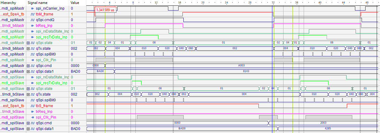
The ClkSync_Prc does the following.
Firstly measurement:
=>source: main/vhdl/modules/common/speA/RxClkSync_SpeA.vhd[tag=ClkSync_Prc_Meas]
    --Check abbreviation rxDataClk in relation to CE4, set shCorr value.
    --
    IF(rxSync_Inp='1' AND rxDataClk_Inp='1') THEN  --dataClk comes, check phase compared with CE
			IF( Q.CE(4)='1') THEN                      --hits exact:
				D.shCorr := Q.shCorr srl 1 ;             -- no correcture, decrease counter resp shifter for corr necessity to "0000"
			ELSIF( Q.CE(5)='1' OR Q.CE(3)='1') THEN    --10 ns error left or right: does not correcture immediately, it may be jittering
        D.shCorr := Q.shCorr(2 downto 0) & '1';  -- correct only if 3x the same.
				D.slower := Q.CE(5);                     -- slower if after CE4. CE4 should be elongated.
			ELSE                                        --else: dataClk is outside CE 5..4..3
			  IF(Q.shCorr /="0000") THEN               -- if the corr counter is not 0, then
				  D.shCorr := Q.shCorr srl 1;            -- wait 1..2 period, do only any 2. or 3. period.
				ELSE
          D.shCorr := "1010";                    --corr immediately (waiting period is expired), set for 2 periods to wait after corr
          IF Q.CE(9 downto 6)/="0000" THEN D.slower := '1'; ELSE D.slower := '0'; END IF;  -- slower if after CE4 to elongate CE
        END IF;
			END IF;
		ELSE        -- Outside of the rxDataClk or outside sync phase, then change nothing.
		  D := Q;   -- hold the value.
		END IF;
    --
If the rxDataCE_Inp clock is exactly synchronous to CE4, it is stable.
An abbreviation because of some disturbance on the line can occur.
Only if at least 3 times one after another the rxDataClk_Inp is one 10 ns left or right,
the only one necessary adjustment is done. Three times after another it is a significant signal
that the clock should be adjusted. Only one or two times, and after them back to exact on CE4,
this is dedicated as only temporary disturbance. This prevents unnecessary CE jittering.
If the clock is outside of the range CE 5..4..3 the adjustment is necessary. But also here the adjustment is not done hectically. Only each forth clock is adjusted. It helps that the mean value of the CE and hence all outputs have a period not outside of 97..103 ns. This helps to prevent jitter propagation.
Secondly actuating:
=>source: main/vhdl/modules/common/speA/RxClkSync_SpeA.vhd[tag=ClkSync_Prc_Act]
    --Executes the correcture on the proper edge of CE8, CE9, CE10
    --
		IF(Q.CE(8)='1' AND Q.slower='0' AND Q.shCorr(3)='1') THEN
			D.CE := "00000000001";              -- faster, switch from CE8->CE0
			D.shCorr := Q.shCorr AND "0111";    --after corr, remaining gap periods without corr.
		ELSIF(Q.CE(9)='1' AND Q.shCorr(3)='0') THEN -- no corr necessity, divide by 10,
			D.CE := "00000000001";              -- normal case CE9->CE0, (do not use CE10)
		ELSIF(Q.CE(10)='1') THEN              -- ELSE: it is slower='1' AND corr(3)='1') THEN
			D.CE := "00000000001";              -- slower , CE10->CE0
			D.shCorr := Q.shCorr AND "0111";    --after corr, remaining gap periods without corr.
		ELSE
			D.CE := Q.CE rol 1;           --CE0->CE1 etc. normal shifting
		END IF;
If the shCorr shift register is set on the 3th position, it is either three times
recognized a 10 ns abbreviation, or the adjustment should be done immediately because of
more abbreviation.
On faster (Q.slower='0')Then after the CE8 the CE0 follows. The CE9 (or CE(9)) is omitted.
It means this CE period has only 90 ns. The CE9 is never used in the design.
If CE9 is activ and no adjustment is necessary (the normal case), CE0 follows.
If an adjustment is necessary it goes to the last ELSIF where CE10 is checked.
This is already the elongation of the CE period to 110 ns. It should follow CE0.
In the case of adjustment the bit 3 of shCorr is cleared.
Together with the shift it creates not too much correcture.
See the image:
-
If the synchronization starts, the
rxDataCE_Inp(yetrxDataClk_Inp) is per accident left of CE0. It means it should be corrected. -
The
shCorris set toA = 1010to adjust immediately, and then adjust one time more in the after next bit. This adjustment is done. You see the nextCE_Out(0)on step more right (10 ns). -
In the next 3 bit times no adjustment follows because the
shCorris not 0. This is the calming time to avoid hectic edges. -
Then again
shCorr=1010(gray) with adjustment and immediately shift, repeated two times.
Then in the mid of the immage nearly the correct CE is reached. Now the fine adjustment comes:
-
The last adjustment is on the
shCorr=B. -
After them the
rxDataCE_Inpis exact. It means by shifting right 3 1 0, no more adjusting occur.
4.6. SpiA - interface to the controller
The SpiA module processes the communication via SPI interface, especially bit shifting.
4.6.1. Inputs and Outputs
I/O for SPI:
=>source: main/vhdl/modules/common/speA/SpiA_SpeA.vhd[tag=InOutPins]
--=================== Signals to ports of the chip:
  spi_MiSo_Pin: IN BIT;
  spi_MoSi_Pin : OUT STD_LOGIC;
  spi_Clk_Pin : OUT STD_LOGIC := '0';
The spi_MoSi_Pin and spi_Clk_Pin are STD_LOGIC because it should be possible to set it in Tristate 'Z' for test approaches.
The spi_MiSo_Pin is always an input, hence BIT is sufficient.
The meaning of this pins should be familiar, see known SPI documentation.
Inputs from other modules:
=>source: main/vhdl/modules/common/speA/SpiA_SpeA.vhd[tag=Inputs]
  --=================== input from other modules:
  spi_Cmd_Inp: IN BIT;  --comes from frame signal on input pin
  spi_reqTxData_Inp: IN BIT; -- comes from TxSpe_SpeA module, after SFD, this module should prepare and offer the txData
  spi_rxDataState_Inp: IN BIT;  -- 1 then sync is reached, all data should be gathered.
  spi_rxData_Inp: in BIT;  --received data from RxSpe_SpeA module
  spi_rxDataCE_Inp: in BIT;  --received data clock enable from RxSpe_SpeA module
-
spi_Cmd_Inp: This is theframe_infrom the controller to trigger reading first two words. -
spi_reqTxData_Inp: This comes from the <<+TxSpe>> module, outputreqDataTx_Out. -
spi_rxData…_Inp: This three signals comes with the receive clock. Thespi_rxDataCE_Inpis the relevant clock enable. Thespi_rxData_Inpis shifted in registers and used for the other logic which switches with the internalCE0-clock enable (100 ns cycle). It means for that only 10 ns (100 MHz central clock) is possible. -
The
spi_rxDataState_Inpcomes in the exact time where data are received, also with thespi_rxDataCE_Inpas validation clock enable, see RxSpe preparing the receive data input from SPE. It controls writing to the RAM via SPI.
Outputs to other modules:
=>source: main/vhdl/modules/common/speA/SpiA_SpeA.vhd[tag=Outputs]
--=================== outputs to other modules:
  spi_cmd_Out: OUT BIT_VECTOR(15 downto 0);    --the command word from SPI after spiCmd
  --data1_Out: OUT BIT_VECTOR(15 downto 0);  --the f irst data word from SPI after spiCmd
  data_Out: OUT BIT_VECTOR(15 downto 0);   --the current data word from SPI while tranmitting
  ceData_Out: OUT BIT;
	ceCmd_Out: OUT BIT;
spi_txD_Out: OUT BIT; --the data bit to Tx via SPE-
spi_cmd_Out: Via SPI a 16 bit command word is read on start of frame and presented here. The bits have special meaning in other modules, see cmd word. -
Todo: more info read via SPI
-
spi_txD_Out: This are the data bit immediately just in time to transmit via SPE. See TxSpe transmit data input to SPE.
4.6.2. Variables of SpeRx_prc: SPE rx data processing
=>source: main/vhdl/modules/common/speA/SpiA_SpeA.vhd[tag=SpeRx_REC]
TYPE SpeRxVars IS RECORD
  ctBitsSpeRx: STD_LOGIC_VECTOR(3 downto 0);
  shDataSpeRx: BIT_VECTOR(7 downto 0);
  dataSpeRxHi: BIT_VECTOR(7 downto 0);
  dataSpeRxLo: BIT_VECTOR(7 downto 0);
	ceData: BIT;
END RECORD SpeRxVars;

SIGNAL qRx: SpeRxVars;
This is for the SpeRx_prc: PROCESS (clk100, CE0):
-
qRx.shDataSpeRx: immediately shift register forspi_rxData_Inp:d.shDataSpeRx := spi_rxData_Inp & qRx.shDataSpeRx(7 downto 1);
-
qRx.dataSpeRx: It stores both bytes ofshDataSpeRxif the bytes are filled. This register is used to transport the data to theshDataSpiin the given time.
4.6.3. Variables of Spi_prc: PROCESS: SPI read and write from and to controller
=>source: main/vhdl/modules/common/speA/SpiA_SpeA.vhd[tag=Spi_Variables]
--====== volatile working FF
TYPE Spi_Variables IS RECORD
  cmd: BIT_VECTOR(15 downto 0);
  data1: BIT_VECTOR(15 downto 0);
  state: BIT_VECTOR(5 downto 0);


  cmdQ: Bit;           --delayed spi_cmd_Inp to edge detection.
  ctBitsSpi: STD_LOGIC_VECTOR(3 downto 0);
  spiBit0: BIT;    -- 1 then the next ct underflows, 0 is reached.
  spiOn: BIT;      --1 then generates spiClk

  shDataSpi: BIT_VECTOR(15 downto 0);   --data read from controller
  testDataSpiRx: BIT_VECTOR(7 downto 0);   --data read from controller
  rxWord1: BIT;   --set on slave to save first lo word as length
  ceCmd: BIT;
  shDataSpeTx: BIT_VECTOR(7 downto 0);
  testDataSpeTx: BIT_VECTOR(7 downto 0);   --it is only for test, not used in the routed FPGA

END RECORD Spi_Variables;

SIGNAL qSpi: Spi_Variables;  -- stateMachine
ALIAS qSpistateIdle: BIT IS qSpi.state(0);  --expected either cmd or carrier
ALIAS qSpistateCmd: BIT IS qSpi.state(1);   --read cmd
ALIAS qSpistateData1: BIT IS qSpi.state(2); --read data1
ALIAS qSpistateData: BIT IS qSpi.state(3);  --read/write data
ALIAS qSpisubstatePrep: BIT IS qSpi.state(4);
ALIAS qSpisubstateMaster: BIT IS qSpi.state(5);
This is for the spi_Prc: PROCESS (clk100, CE0), see Process spi_Prc
-
qSpi.shDataSpi: shifted in bits from SPI read -
qSpi.shDataSpeTx: shifted out bits for Tx
4.6.4. Process spi_Prc
This processes the read data from SPI: SPISOMI.
Note that the FPGA is the SPI-Master, it offers the SPICLK.
Hence this process determines the SPICLK output too.
It is a concurrent process because it shold work twice in the 100 ns basic cycle:
The SPICLK is produced on qSpi.spiOn and comes with the shown CE signals.
=>source: main/vhdl/modules/common/speA/SpiA_SpeA.vhd[tag=spiClk_Prc]
-- Output SPI clk with CE2..7
--
spiClkHi_Prc: PROCESS (clk100, CE2, CE7) begin IF ((CE2='1' OR CE7='1') AND rising_edge(clk100)) THEN
  IF( qSpi.spiOn ='1' AND CE2 ='1') THEN
    spi_Clk_Pin <= '1';        -- spiClk: positive leading edge after CE2: data request to controller,
  ELSE
    spi_Clk_Pin <= '0';        -- negative falling edge after CE7: controller latches the data.
  END IF;
END IF;  END PROCESS;
The Spi_Prc runs all with the CE0 clock enable signals.
It means all Flipflop of the Spi_Variables have 100 ns possible delay to switch
as timing constrain in the FPGA:
=>source: main/vhdl/modules/common/speA/SpiA_SpeA.vhd[tag=spi_Prc_Start]
--SPI read and write from and to controller, one shift register shDataSpi for both.
--
spi_Prc: PROCESS (clk100, CE0)
  VARIABLE d: Spi_Variables := qSpi;   --default values same as q, means hold, don't change.
  ALIAS dstateIdle: BIT IS d.state(0);  --expected either cmd or carrier
  ALIAS dstateCmd: BIT IS d.state(1);   --read cmd
  ALIAS dstateData1: BIT IS d.state(2); --read data1
  ALIAS dstateData: BIT IS d.state(3);  --read/write data
  ALIAS dsubstatePrep: BIT IS d.state(4);
  ALIAS dsubstateMaster: BIT IS d.state(5);
BEGIN IF (CE0='1' and clk100='1') AND clk100'event THEN
  d.cmdQ := spi_Cmd_Inp; -- OR spi_rxCarrier_Inp; --start condition for SPI activity, detect edge 0->1
  --
  IF( clr = '0'   --clr is lo active
    OR qSpi.state = "000000" ) THEN
    --=== Only first time on start with 0 or on clr
      dstateIdle := '1';
      d.data1 := x"FFFF";   --on non initialized slave, first data high byte is sender identification
      d.cmd := x"0000";     --default
This start block shows also the reset condition: Either the clr input is given or all states are zero, condition on hardware reset.
This process reads the data via SPI and shifts it into the qSpi.shDataSpi register:
IF(qSpi.spiOn ='1') THEN
  d.shDataSpi := qSpi.shDataSpi(14 downto 0) & spi_MiSo_Pin;
END IF;
It shifts the data bit to left to MSBit, first read bit lands in the MSbit after 16 shift operations. This is correct if the SPI interface on the controller is programmed to shift out first the MSB most significant bit for 16 bit access. This is supported by probably all controllers. The 16 bit access should be used to reduce effort on the controller (byte access needs double number of accesses). Shift out first MSB and not LSB was the originally intension from SPI. SPI is not standardized, it is only a "quasi standard". Hence this modus is used here as only one. More modifications seems to be unnecessary. See also chapter Endian approaches: Ethernet Big endian LSB first, SPI: word access, MSB first
To transmit this data it should be shifted in the requested order for the Ethernet bit order rules:
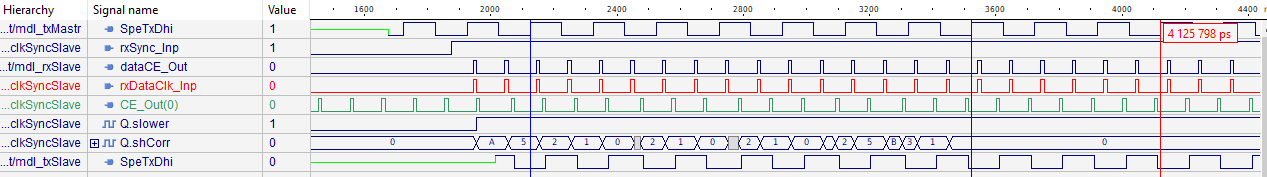
4.6.5. Sequence cmd and data between controller and FPGA/SPI
The sequence for the master starts with the frame_inp of the FPGA, here in the simulation tbM_frame,
red line. This signal is compared with the qSpi.cmdQ, line below, to detect the leading edge.
The trailing edge has no meaning. The leading edge of the frame_inp is Hi→Lo.
After this the SPI reads from the controller 2 * 16 bit, one for cmd, the next for the first data.
It is seen on spi_Clk_Pin.
The result is the set to
-
qSpi.cmd: It changes from0000toA003, and to -
qSpi.data1, changed fromBAD0to8143(only as example data).
Both values remain in the register, also for the next cycle, because the same values are read in any cycle. That is typical for the application software.
To compare with the sequence on slave:
In the left telegram the slave has no frame_inp, the signal tbS_frame remains on hi.
This is given in practice if the slave controller is not programmed yet.
But for the second telegram in this image tbS_frame comes.
Meanwhile (possible sometime later) the slave controller is synchronized in its interrupt
to the SPE data stream, has initialized the SPI interface in the controller
and produces the frame_inp signal typical via a PWM output (pulse width modulation).
The time synchronization between the SPE data stream and the PWM module and the interrupt
to program the SPI interface is done with the signal spi_rxDataState_Inp
which is the same as dataState_Out from the RxSpeA module
driving the pin frame_out to the controller.
Independent of telegram content and SPI communication, the frame_out to the controller
can be used for synchronization with a PLL control software (Phase Look Loop).
This is a necessary condition for the Ring topology in a fast cycle,
because the cycle of SPE communication and the interrupt cycle in the controller
to initialize the SPI communication and read and write data should be synchronized.
There is no "telegram stack" in comparison to an ordinary Ethernet adapter
which does not support such an fast data exchange.
For the slave in the second (right) telegram, now the cmd and data1 are read via SPI.
The cmd changes from 0000 (initial) to for example here 2003.
It determines furthermore acting as slave.
The data1 changes from BAD0 to for example here 4203. That is the sender address.
In the master FPGA the signal txReq_Inp comes in that moment, if the cmd bit 13 is set.
This is a signal used in the TxSpeA module. For the next telegram (right side)
this signal comes immediately with the frame_inp, this is the red tbM_frame.
This is the normal sequence for the master: With frame_inp the transmission sequence starts.
But: Because also with frame_inp firstly the FPGA should read the cmd and data1 via SPI,
the signal spi_ReqTxData_Inp is delayed in the TxSpeA module, see TxSpe transmit data input to SPE.
The TxSpeA module waits a definite time for reading the both data words for cmd and data1
via SPI.
In the moment where spi_ReqTxData_Inp comes the TxSpeA starts with transmission
of the SFD start frame delimiter and the first data1 word. This is loaded before,
it is a constant data word with usual the same content for all telegrams,
it is the sender identification and the length of the datagram.
Now, after spi_ReqTxData_Inp the SPI start working with furthermore accesses to the controller
for the following data words. But this access is fine tuned between the timing to transmit
via SPE. the timing of receive in the RxSpeA module (should write via SPI) and the SPI timing.
For that the short state substatePrep is set (number not visible, between 01 and 08
in the green line qSpi.state).
For that a code snippet from SpiA_SpeA.vhd:
=>source: main/vhdl/modules/common/speA/SpiA_SpeA.vhd[tag=spi_Prc_reqTxData]
    ELSIF( spi_reqTxData_Inp='1') THEN  --STATE 1->18  should deliver Spi_TxD to Tx_TxD
      dstateIdle := '0';              --Note: spi_rxDataState_Inp will behandled in
      dsubstateMaster := NOT spi_rxDataState_Inp;  --it is 0, slave if spi_rxDataState comes similar, not later.
      d.rxWord1 := spi_rxDataState_Inp; -- used to set length of telegram form first received word
      dstateData :='1';
      dsubstatePrep := '1';
      d.shDataSpeTx := qSpi.data1(15 downto 8);     -- load 1. data word to SpeTx
      d.testDataSpeTx := qSpi.data1(15 downto 8);   -- only for test, not used in FPGA
      d.shDataSpi := qSpi.data1;  --as first word write data1, hint: bit 7..0 used for shDataSpeTx later
      d.ctBitsSpi :="0111";       --time till start spiClk. Only 7 is admissible, correct time to reload
This time fine tuning depends on shift and bit approaches, see next chapter.
The signal spi_reqTxData_Inp (light green line) comes from the module TxSpe transmit data input to SPE
-
in the master either as time condition after the SFD output (start frame delimiter). On master the request from tx comes at last from the
frame_inpsignal, heretbm_frame. -
or in the slave in the moment of receiving the SFD bit. This is seen in relation of the signal
spi_rxDataState_Inpto the signalspi_reqTxData_Inpon the slave. On slave the request for tx comes from the received signal.
Both conditions indicate the need for new data. Hence the SPI communication starts
seen with the spi_Clk_Pin after the correct time.
For the first telegram of the slave it hits an uninitialized SPI interface on the controller.
It means the controller may not react for the spi_Clk_Pin and the spi_SoMi pin
delivers a 0 signal. But this is not used in that state.
In the second telegram of the slave all is prepared, as well as on the master.
On the master the signal spi_rxDataState_Inp comes a while after starting trasmission
via SPE, here seen on the SPI clock or on the qTx.state.
This is the echo in the Ring after all station passing. It is important to consider
this relations too: The storing of received data is executed via SPI too, with the same clock.
For the slaves that relations are proper:
Storing received data and reading the next data to send is anyway hard synchronized,
because the received data determines the SPE acitivity and the send data follows this.
But on the master the send of data is primary for the SPI activity. The received data comes any time later. The received data should be aligned to the SPI bit shifting correctly. Then the data are stored not in the first prepared RAM locations, it is not possible, but in later locations. One 16 bit word needs 1.6 µs. Delay in the ring between two station is, seen here on the SPI clk time between master and slave, approcimately 0.3 µs. It means if 10 station are in the ring, about 3 µs delay for the echo on the master. It means also that the SPI clock should work for at least 2 or 3 data words more as necessary for transmission data, to store the received data, on the master.
4.6.6. Shifting data to Tx, timing
The SpiA module prepares the data reading via SPI completely down to the bit to transmit,
offering on spi_txD_Out pin of this module.
Shifting the data to transmit and provide the data bit in the correct time (clock cycle)
is task of this SPiA module.
The module TxSpe transmit data input to SPE offers the start signal for transmission:
spi_reqTxData_Inp as input on SpiA, output on TxSpeA: reqDataTx_Out.
This signal determines starting the SPI access.
The second task for SpiA is shifting and storing the data from the module RxSpe preparing the receive data input from SPE
to write to the controllers RAM. The data comes to the spi_rxData_Inp input of the SpiA
from the RxSpe module:
-
On a Slave for Ring Topology this data are in the same correct timing sequence , because the receiving data determines the timing and hence the reading of transmission data. Note that generally there is only one SPI access to read and write data, of course from and to different addresses in RAM, but with the same SPI clock signal using the SPIMOSI (master out slave in) to write and similar SPISOMI (slave out master in) to read.
-
But for the master in Ring topology receives this data as echo through the whole Ring, sometimes later. The delay is …3 µs for 10 Stations in the Ring. Additional there can be a jitter.
-
The first approach for that is: The data should be stored with 16 bit to synchronize data writing with the correct bit, so that receiving data are correct aligned in the RAM.
-
For that more as 16 bit are not stored. It means on greater delays in the Ring the first written data of SPI (first 1..3 words) are not come from receiving. They are not valid. Hence first
0xffffare written instead received data, after them the real received data. -
To recognize this in the controller’s software the first data can be distinguished from the really first received data word. This is done by the value
0xFFFFfor this first words.
-
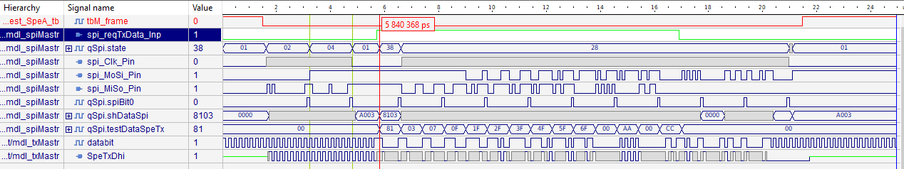
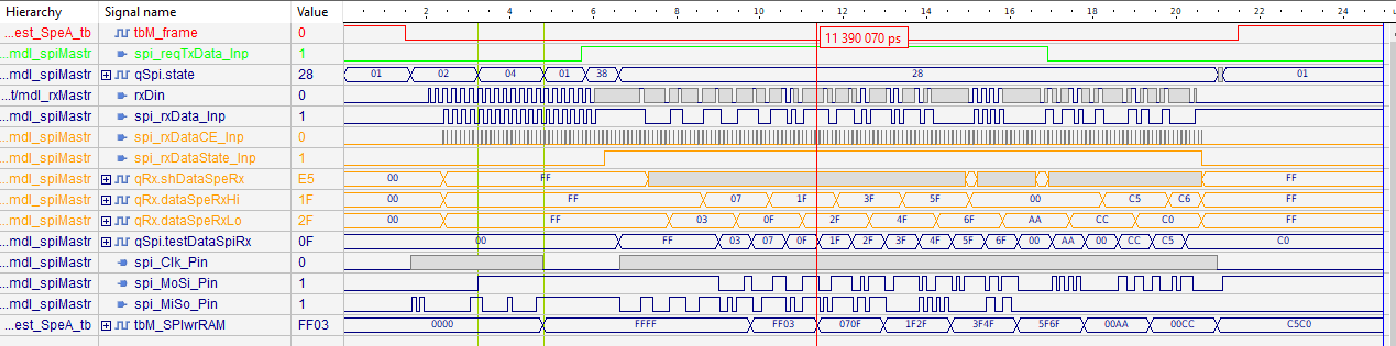
This first image as test Test_SpiShDataTxMastr.awc result shows a master in the Ring topology and an uninitialized slave.
The communication in the ring, forwarding data, should be also proper
if a slave station is not working in the moment.
-
The sequence for the master starts with the
frame_inpof the FPGA, here in the simulationtbM_frame, red line. This signal forces immediately reading of two data words, the command word and the first data word. See also chapter above: Sequence cmd and data between controller and FPGA/SPI. -
After a determined time to read the first data words, the signal
spi_reqTxData_Inp(light green) comes from the TxSpe module to the SpiA module. Immediately with this signal the module TxSpe transmit data input to SPE starts output the Start Frame Delimiter SFD as end of the sync pattern and afterwards the first data word, which is already stored. -
The
qSpi.statechanges from01 = idleto38 = master + dataPrepone CE-clock later. The state machine switches with the CE0 clock enable (100 ns cycle). This state waits exact 8 CE cylces = 8 bit times, then switchesqSpi.stateto 28 = master data. -
In this state 28 = master data the SPI clock comes and reads and writes data from and to the controller, see signal
spiMastr.spi_Clk_Pin. -
For the master this first data to write are
0xffffbecause nothing is received till now. It is seen onspiMastr.spi_MoSi-Pin. -
But for Tx the next data are read, see
spiMastr.spi_MiSopin. This is the second data word. The first data word was reading in the first SPI_CLK phase into 'data1' already and it is shifted out via SPE. -
This next data are shifted in to
spiMastr.qSpi.shDataSpi. In the image you see only a gray bit stream, it is working. But in the next track inspiMastr.qSoi.testDataSpeTxyou see a snap shot after 8 shift operations. The data to transmit comes always from the high byte from SPI. Hence you see8103from the first data word, and then070F1Fetc. which are all read from the RAM gotten viaspiMastr.spiMiSo_Pin. You can follow the serial signal on this pin and the shifted result after any 8 bit. Note that SPI reads the MSB bit 15first.
+ See code snippet:
=>source: main/vhdl/modules/common/speA/SpiA_SpeA.vhd[tag=spi_Prc_DataBitMid]
    -- === Handling of data bits ================================================================================
    -- Handling is only necessary in the mid and on end of a spi word.
    IF ( qSpi.ctBitsSpi = "1000") THEN             --==== in the mid of ctBitsSpi, proper to 8 bit shifted out with shDataSpeTx
      IF ( qSpistateData ='1' ) THEN            --==== stateTxData
        d.shDataSpeTx := d.shDataSpi(7 downto 0);
        d.testDataSpeTx := d.shDataSpi(7 downto 0);
        d.shDataSpi(15 downto 8) := qRx.dataSpeRxLo;
        d.testDataSpiRx := qRx.dataSpeRxLo;
        IF(qSpi.rxWord1 = '1') THEN
          d.cmd(7 downto 0) := qRx.dataSpeRxLo;  --determines the telegram length from received data word, it is received from master in Ring.
          d.rxWord1 := '0';
        END IF;
      END IF;
-
The
testDataSpeTxare only for visualization, there are removed in the FPGA design. but at the same time also theshDataSpeTxare loaded with that value. And this are the data to offer to the module TxSpe transmit data input to SPE to transmit. But you see exactly this data serial intxMastr.databit. This is the data bit immediately before Manchester-2 coding, which is outputed. Note that on SPE the Ethernet standard is used which means output LSB first, but with big endian.
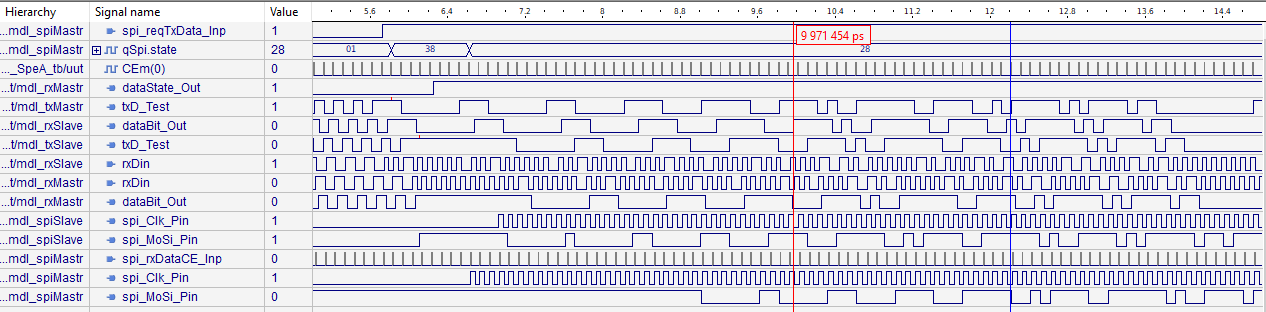
4.6.7. Handling of received data in the Ring-master for SPI-shifting
The first image shows handling received data in the master of Ring topology. This is appropriate to the chapter above for getting transmission data with the same SPI access. It is the same simulation running, only showing other signals.
The SPI sequence is controlled by the spiMastr.spe_reqTxData_Inp
because the transmission data should be read just in time.
This is valid also for Master and for slave of Ring topology.
-
Hence this sequence starts as in chapter above with
spiMastr.spe_reqTxData_Inp, green line. -
The signals from the receiver module RxSpe preparing the receive data input from SPE
spiMastr.spi_rxData*(next tracks) comes asynchronous with the receiver clock:rxDataCE. This receiver clock can have any phase position in comparison with the CE0 clock enable. That is true for the master. In the slave it is synchronized. -
The receiving signals are shifted with the receiver CE in an extra PROCESS
SpeRx_Prc. Hence this Flipflop (FF) group has a possible timing contrain as the Module RxSpe, with 70 ns between received data and this shifting FF. You see the shifted results inspiMastr.dataSpeRxHi/Loin 16 bit but separated to two register. -
The
spiMastr.qSpi.testDataSpiRxare that data which are loaded in the SPI shift register. That timing is determined by the transmission data and clock enabled with the transmissionCE0signal. See the following code snippet:
=>source: main/vhdl/modules/common/speA/SpiA_SpeA.vhd[tag=spi_Prc_DataBitMid]
    -- === Handling of data bits ================================================================================
    -- Handling is only necessary in the mid and on end of a spi word.
    IF ( qSpi.ctBitsSpi = "1000") THEN             --==== in the mid of ctBitsSpi, proper to 8 bit shifted out with shDataSpeTx
      IF ( qSpistateData ='1' ) THEN            --==== stateTxData
        d.shDataSpeTx := d.shDataSpi(7 downto 0);
        d.testDataSpeTx := d.shDataSpi(7 downto 0);
        d.shDataSpi(15 downto 8) := qRx.dataSpeRxLo;
        d.testDataSpiRx := qRx.dataSpeRxLo;
        IF(qSpi.rxWord1 = '1') THEN
          d.cmd(7 downto 0) := qRx.dataSpeRxLo;  --determines the telegram length from received data word, it is received from master in Ring.
          d.rxWord1 := '0';
        END IF;
      END IF;
-
This is the same code snippet shown in the chapter above for tx. The line
d.shDataSpi(15 downto 8) := qRx.dataSpeRxLo;
is the essential for receive data. The assignment form the one FF group
qRxto the FF group of this PROCESS has a maximal timing delay of 10 ns, the system clock of the FPGA, because both clock enable are not related. In the image you see thetestDataSpiRxset in the same time. -
The other byte is handled by:
=>source: main/vhdl/modules/common/speA/SpiA_SpeA.vhd[tag=spi_Prc_DataBitHi]
      -- ==== stateData: finish or load next data
      ELSIF ( qSpistateData ='1' ) THEN           --===== STATE 8:
        IF ( spi_reqTxData_Inp='0' AND spi_rxDataState_Inp ='0') THEN
          dstateIdle := '1';
          d.spiOn := '0';                        -- finish
        ELSE                                     -- get next dataSpeTx from spiRd
          d.shDataSpeTx := d.shDataSpi(7 downto 0);
          d.testDataSpeTx := d.shDataSpi(7 downto 0);
          d.shDataSpi(15 downto 8) := qRx.dataSpeRxHi;
          d.testDataSpiRx := qRx.dataSpeRxHi;
        END IF;
-
It is a part of handling after a 16 bit border. The statemens are similar as handling on the middle of the shifted word above, only the other half word of
qRx.dataSpeRxHiis used. The dispersion between high and lo word also for Tx comes from the rule that Ethernet shifts out first the LSBit and SPI shifts first the MSbit, but both from the high byte (big endian).
The moment where the shifted data from Rx (orange) are used for shifting in SPI depends on the time delay between start transmitting and the moment of receiving. It is undefined and can jitter. Hence the receiving data are stored with 16 bit to get it in any moment.
4.6.8. Handling of received data in the Ring-slave for SPI-shifting
The algorithm are the same, it is not distinguished between master and slave. But the conditions are different.
For the slave in Ring topology the first data byte is already received via SPE and can written via SPI. For that see on the
…TODO more simulation results available, also with different stimuli using the StimuliSelection tool.
5. Functionality over all modules
5.1. Real scope of data signals Master and Slave
D15: slave-a-A46: frame_out
D14: Infineon calctime
D7: Mastr-q-A28: test1_Out spi_TxD 11111
D4: Mastr-J-A22: rxDataState_Out
D8: Mastr-r:B22: test2_Out Tx_TxD = tx.txD_Test (output before manchester-coding)
D10: Slave-t:A27: dataRx_Out : rxSpe*_dataBit_Out = Spi.spi_rxData_Inp
D11: Slave-r:B22: test2_Out Tx_TxD = tx.txD_Test (output before manchester-coding)
D9: Slave-N:A24: SpeRxD2_out_T: SpeRxD2_Pin = exSpe2.rxDin Input after Diff-Pin
D1: Mastr-N:A24: SpeRxD2_out_T: SpeRxD2_Pin = exSpe2.rxDin Input after Diff-Pin
D5: Mastr-t-A27: dataRx_Out = rxDataBit = rx*.dataBit_Out  spi.spi_RxData_Inp = TxSpe.rxDataBit_Inp
D12: Slave-e-A38: SPI CLK
D13: Slave-c-B33: SPI_MOSI
D6: Mastr-p RxCE
D3: Mastr-L-A23: SPI CLK
D2: Mastr-c-B33: SPI MOSI
D0: Mastr-b-B35 frame_in ( from TI)
The following data are transmitted:
Master: 8103 070f 1f2f 3f4f 5f...
Slave:  FF03 070f 1f2f 3f4f 5f ...
-
The left cursor is on D10, Slave dataRx_Out. It shows 11110100 = 2F lSB first. It is in slave, you see above and below the same pattern.
-
The right cursor is on D2, Master SPI data. It shows 00101111 = 2F, MSB first. It is the adequate Byte received on master.
This is the adequate simulation result, src/test/Lattice_pj/Test_All_SpeA/Test_DataBitScope.awc:
Hint: the simulation shlould be executed with 0 delay rxMd0 in Select Stimuli.
5.2. Time stamp and Ring Cycle Synchronization
5.2.1. Standard time stamp approaches
For Ethernet with >= 100Mbit/s there is a NTP "Network Time Protocol" (https://en.wikipedia.org/wiki/Network_Time_Protocol) or better PTP (Precision Time Protocol) (https://en.wikipedia.org/wiki/Precision_Time_Protocol) can be used, accordingly to the TSN (Time Sensitive Network) rules (https://en.wikipedia.org/wiki/Time-Sensitive_Networking).
But this technologies works only for the connections >= 100 Mbit/s, because they are not regarded in the original Ethernet 10 Mbit/s topology. The problem of the originaly 10 Mbit/s Ethernet was: The time of transfer of a telegram depends on the status of the line. For the line a Bus Topology is used. It means all station attacks the line. It is deterministic for transmission in a time range in milliseconds, regarding displacement mechanisms, but not for exact time stamps. Due to the presence of the star topology with its continue data stream, which can work with TSN and PTP, a proper time synchronisation for the 10 Mbit/s where never developed.
Now with SPE also the Bus Topology is in focus, with the so named "Multidrop Technology", and that does not support the time synchronization yet and per default.
But, the Ring Topology offers another approach for Time Synchronization:
-
Prior, not the time stamp should be offered to all stations as accurate as possible, but:
-
All stations should work synchronous.
It means the stations in the ring have the same time, but they don’t know (need not know) the exact absolute time. They work together, out of a global time.
It is possible to insert this stations in a global time (UTC, master clock etc.), but this is task only of the master in the Ring Topology. The master can do so by using one of the possible approaches: Standard Ethernet with TSN and PTP or NTP, or specific variants of SPE (with higher bit rates and Star Topology), which also supports TSN, NTP, PTP. Then the master can forwarding this absolute time in the Ring to all other stations with the Ring Cycle Synchronization, described following.
5.2.2. Ring Cycle Synchronization - approach
The approach of the Ring Cycle Synchronization is:
All Stations in the Ring should work synchronous. It means
-
they have an synchronous interrupt cycle (or a hardware interrupt of the processor),
-
initialize the SPI for data communication with SPE with this FPGA approach,
-
expect an receive telegram to a proper time, necessary after the SPI initialization (in Slave mode) and send it forward to the next station.
-
The master in ring transmits its telegram to an expected time.
-
A PWM (Pulse Width Modulation) often use for output of data, for example Firing pulses for power valves or also simple outputs should work exact synchronous in this cycle to refresh the current data in each cycle.
-
The average time for Measurements should exact follow this cycle. For Measurements always the middle value (average, integral) of the pre-period should be used as characteristic of input signals, not a accidently time for a fast measurement. This is necessary to suppress technical noise which is usual synchronous to the actuator period (from a PWM), or also, to suppress accident disturbance with a higher frequency as the measurement one.
This is all necessary for example in control of electrical signals.
The cycle for this can be for example 50 µs, as also a little bit longer if possible, … 1 ms.
The goal is: Do that with a jitter less as possible and/or necessary.
In the Ring cycle the time stamp existing in the master can be forwarded to all slaves if they need an absolute time for processing. But often only the master may need this.
5.2.3. Solution frame_in/out and PLL
The master should transmit the telegram starting with the frame_in hardware signal.
This signal can/should be produced in the controller by a PWM output.
The PWM with the time of the master determines the time of transmission.
On frame_in on master first the preamble with sync bits are transmitted.
After a determined number of sync bits, hence a determined time,
the SFD Start Frame Delimiter is sent, after them the data.
The first slave in the Ring receives firstly the sync bits.
During the sync bits the Slave tunes its central CE clock enable signal due to the
sync bit edges (the dataCE_Out of the module RxSpe preparing the receive data input from SPE.
This is done in the module Synchronization of the internal CE clock to the signals from outside.
It means on receiving the SFD the clocks are synchronized already.
With the SFD the signal frame_out is produces as output of the FPGA
to use as input to the controller.
This signal has a minimal jitter doe to the clock sync capability (measured 30 ns)
and a known delay.
With the frame_out as input to the controller either an interrupt to process the data
can be start.
Or better, an internal PWM can be controlled by a PLL (Phase Look Loop) algorithm,
see next chapter.
In both case the interrupt starts synchronous (using PLL before receiving the SFD,
force an interrupt immediately after the SFD).
This interrupt can put and get data to and from the RAM
where data for SPE are written and read (via SPI).
It means the data exchange are also related to the ring cycle.
Always new received data are processed and always new processed data are transmitted.
Of course this data timing should be tuned to the telegram timing.
The next slave stations in the Ring receives the SFD in a time which is exact related
to the receive moment in the Slave before, because the transmission is done with the
central CE clock, which is synchronized to the dataCE_Out of the receiver module
with measured 30 ns jitter.
But because the jitter may be added, the next station has a jitter with double spread, but with a Gaussian normal distribution, because the jitter between one station may be seen as accidently. Due to the real clock frequencies, beating can also occur. All in all the jitter is one step greater to the next stations. On 10 stations 300 ns jitter is expectable. But this is not too much.
The jitter can be reduced between each cycles even by the PLL control.
5.2.4. PLL control of the interrupt cycle
The solution of PLL control is individual for different controller. The principle is:
-
Measurement or capture of the time where the
step_inis occurring, as relative time (value of a wrapping counter). -
Comparison of this time information with the time information from the same source where the interrupt is forced. This is very simple if the interrupt is forced by the same timer reaching the zero-value as the capture of
step_inis done. -
Adjusting of the timer for the interrupt due to the measured difference. Whereby not the exact measured differenc is used for the new value. This is a simple P-part-controller. It is better to have a real PI controller (Proportional and Intergral Part) which is changed by the time difference as input. The output can be used as reload value for the timer, which generates the interrupt.
It means while PLL controlling the interrupt cycle is a little bit lesser or greater, not constant with the same reload value. A constant cycle has usual not the same time as in the master cycle because of quartz frequency tolerances. It would run away by accumulation of time. Hence the time should be adjusted sometimes a little bit.
The different length of an interrupt cycle is a jitter between the Ring cycle (telegram cycle) and the internal timer and interrupt. The range of this jitter depends on the resolution of the timer. If the timer both for interrupt and capture runs with 10 MHz only (100 ns), then the jitter is of course > 100 ns. Because of some small inaccuracies the jitter may be in range of 300 ns. This is added to the telegram jitter (from 30 ns in the first station to 300 ns in the 10th station). A sum of 600 ns jitter for a 50 µs interrupt cycle is not too far. But for analog measurement and also for the PWM output this can be on a limit.
Another possibility for synchronization of the controller with the Ring cycle is:
Using a 10 MHz or 5 MHz output signal caused by the internal central CE clock as clock input
for the processor. Processors often has a PLL for the internal clock to generate a higher
clock frequency from a Quartz with lower frequency.
If the FPGA output is used as clock input for the controller,
the controller has not an own abbreviating Quartz frequency, and the PLL is not necessary.
Measurement the time of frame_in should be used only for the first synchronization
and also for checks.
For this solution it should be known that the 10 MHz or 5 MHz clock output can have abbreviations from the contant frequency because of the clock synchronization Synchronization of the internal CE clock to the signals from outside in the FPGA itself. The CE period switches between 9..10 internal clock periods (90..100 ns) or between 10..11 (100 .. 110 ns). This unrest should be processed by the controller’s PLL.
Hence the best solution is: The FPGA clock itself does not come from the Quartz, it does come from a PLL in the FPGA. Then each FPGA can be synchronous to the master’s quartz frequency. And also, the controller in the master is forced by the FPGA quartz or vice versa (maybe better). Hence only one quartz frequency exists in the whole ring. All is synchronous in one ring. Another related ring can be used also the same controller quartz if it is mastered by the same controller. This is the best solution of exact cycle synchronization.
Because of the cycle synchronization so far as possible all stations have the same time, independent whether they use (and knows) the time stamp itself or not.
5.3. Data exchange between the application in the controller and the FPGA via SPI
The data exchange is the important interface between FPGA-PHY and the controller.
5.3.1. Timing with step_in and SPI data for the SPE-Master
The trigger for the data exchange on master is the frame-in Signal on FPGA. This is produces per hardware by for example a PWM output, see Chapter Solution frame_in/out and PLL.
The FPGA is the master for the SPI communication.
It means, the FPGA as SPE-master starts the SPI data exchange immediately after the frame_in.
To resolve this SPI transfer the controller have to be initialized for SPI-data transfer before the frame_in signal comes.
For the timing for a cyclic interrupt it means, firstly the initialization of SPI-transfer should be done.
The moment to do depends on the programm stepping (machine codes) and should not jitter too much.
The frame_in signal should be produces by a PWM hardware (puls widht modulation)
which should be part of a controller.
Then the moment of output the falling edge of frame_in can be tuned by the compare value
of the PWM. It can be tuned in software, but the value should be fixed in run time.
Now after frame_in leading falling edge, the SPI should output the data.
It depends of the controller how does it work. Tip: Use 16 bit per data word.
Often either a FIFO (fist in first out) register is part of the SPI interface in the controller,
or DMA (direct memory access) can be used, or both in combination.
For FIFO the data which should be read from the FPGA should be written into the FIFO register structure
before the frame_in edge comes.
For DMA the DMA controll registers should be initialized for this cycle before the frame_in edge comes.
For both, both should be initialized.
The fast image should show the timing
------ccciiiiiiccccccdddccccccccccDDDccccccccccccccccc--------------- ohne cycle interrupt
++++++++++++++++++|______________________|++++++++++++++++++++++++++ The PWM output for frame_in
-
The
cccshould present any statements of the cyclically interrupt -
iiiare the initializing statements for SPI, programming FIFO and/or DMA. -
dddare data which are calculated on the fly for transmitting, possible, see next -
DDDare data which are used on the fly from the SPE communicaiton, see next. -
|___|should present the hardware signal forframe_in, be carefully with the moment of edge.
5.3.2. Timing with step_in and SPI data for the SPE-Slave
On the slave the timing should be similar. But not the step_in is the trigger,
the data comes with receiving a telegram.
Exactly therfore SPE-master and SPE-slave should be synchronized in the cycle time,
see chapter Ring Cycle Synchronization - approach. Then the receive telegram does not come unexpecting,
it comes in the expected time range.
Before the receiving is expected, also (as in SPE-master) the SPI interface of the controller should be initialized. All other is adequate.
5.3.3. Data on the fly
As shown in the graphic it is possible to write data for DMA transfer a little bit shortly before they are read from SPI to transmit. The same is with receiving: Using immediately after receive.
But this requires that the timing both from machine code execution in interrupt and the position of data in the SPE telegram are known, stable and tuned. For some simple controlling applications this can be done (need constant calculation time, less jitter). Hence the dead time in the controlling cycle can be reduced. But this is a possibility which can be used in response to the application. You should also regard, that FIFO data should be written (and hence known) before the telegram starts, only DMA data can use this possibility.
In all cases it is not possible to handle the SPI data in software. For that the data rate is too fast (10 Mbit/s, 1.6 µs for 16 bit).
For receiving it is similar. Using a FIFO the first data are written in the FIFO, but some times the FIFO size is too small, and the FIFO is entlees via DMA to the RAM. Then this just in time data can be used. For just in time performance either no FIFO capability should be used or with less size. The DMA should be prior and fast enough for 1.6 µs per access (16 bit SPI access, 10 Mbit/s).
5.3.4. Meaning of the data words
The first data word (16 bit) is used as command as described in …TODO. The second data word is the sender address. All other data words are user specific, payload in the telegram.
The user should have a data struct (C-language, also in C++),
which contains the whole data for SPI beginning with the command and sender word
as int16, following by the user data.
5.3.5. Received data, meaning
The received data are written via DMA to the RAM. The first two words contains the own command and sender, then received data with the sender address follows. Between both they may be fill words with content 0000 on the SPE-master if the response time in the ring is a little bit greater.
5.4. Endian approaches: Ethernet Big endian LSB first, SPI: word access, MSB first
But the output on SPE is defined adequate to the Ethernet standard with first output the LSB, but from the high byte of the 16 bit access (big endian approach).
The big endian approach should be correct understand: If a memory word (16 bit) is accessed, the processor reads the memory word correct. There is no endian approach for reading whole words from memory, endian approach is only existing for serializing of a word. It means the 16 bit access for a 16 bit word is always correct independent of endian thinking.
But for a 32 bit word, which is accessed by two 16 bit reading from SPI,
first the bits 31..16 should be accessed from memory to transmit exactly first bit 24..31 and then bit 16..23
via Ethernet SPE. Following with access bits 15..0 via SPI to transmit bits 8..15 and then 0..7 via SPE.
To do so, it is necessary to reverse the content in the memory.
This is similar the known hton and ntoh operations "host to net" and "net to host".
But, for approaches of fast data transfer often only 16 bit are used. The order of word remains independent of big or little endian accesses. And, if both partner accepts a 32-bit or longer word without word swapping, it is also okay. The swapping is only necessary if the information are evaluated in an unknown or common way, then the big endian approach is valid and should be recommended. This is an effort in software, not in the PHY layer of this FPGA.
Examples to explain the big endian approach:
 //data example:
 int16 data = 0xabcd;
 int16 datb = 0x1234;
 int32 dat32 = 0xfe0a5678;
Memory content:
  cd ab 34 12 78 56 0a fe      content in memory as byte width for little endian approach
  abcd  1234  5678  fe0a       content in memory 16 bit width for little endian approach
  abcd  1234  fe0a  5678       changed content to transmit for big endian approach
  ab cd 12 34 12 fe 0a 56 78   Transmit order, transmits LSB of each byte first.